"DDR4 SPD 标准协议:优化内存通道初始化与优化的关键信息"
需积分: 48 122 浏览量
更新于2024-01-30
6
收藏 1.6MB PDF 举报
DDR4 SPD标准协议描述了所有DDR4内存模块的串行存在检测(SPD)值。SPD数据提供了有关内存通道上所有模块的关键信息,并旨在由系统的BIOS使用,以便正确地初始化和优化系统内存通道。为了允许最大的灵活性随着设备的发展,本文档中描述的SPD字段可能支持设备配置和不包括在JEDEC DDR4 SDRAM数据表(JESD79-4)中的计时选项。此外,由于SPD EEPROM的存储容量有限,因此采用了多种技术进行优化这些字节的使用,包括覆盖和运行长度有限的编码。
根据JEDEC标准21-C,发布30页4.1.2.L-6 - 1,JESD 21-C章节标题:L附录:DDR4 SDRAM模块的串行存在检测(SPD)委员会文件参考标题:DDR4 SPD文件发布6,设备类型标识符UDIMM修订1.3,RDIMM修订1.4,LRDIMM修订1.5,NVDIMM-N修订1.3。
串行存在检测(SPD)是一种重要的协议,用于描述DDR4内存模块的信息。SPD值包括设备类型标识符、修订版本以及其他关键信息,以确保系统能够正确地识别和初始化内存模块。此外,SPD还提供了关于内存通道上所有模块的详细信息,以帮助系统BIOS正确优化内存通道。
由于SPD EEPROM的存储容量有限,因此需要采用多种优化技术来节省空间。其中包括覆盖和运行长度有限的编码,以确保在有限的存储空间内存储尽可能多的关键信息。这些优化技术使得SPD数据能够在占用较少的存储空间的同时仍提供必要的关键信息。
此外,为了允许最大的灵活性,SPD字段可能支持设备配置和不包括在JEDEC DDR4 SDRAM数据表(JESD79-4)中的计时选项。这意味着DDR4内存模块可能具有各种配置和计时选项,而这些选项可能不在标准数据表中列出,因此需要通过DRAM供应商资料表或JESD79-4来确定组件的兼容性。
总之,DDR4 SPD标准协议对所有DDR4内存模块的串行存在检测(SPD)值进行了详细描述,提供了关键的信息以帮助系统正确初始化和优化内存通道。通过优化存储空间和支持设备配置和计时选项,SPD协议为DDR4内存模块的灵活性和兼容性提供了重要保障。
JEDEC Standard No. 21-C, Release 30
Page 4.1.2.L-6 – 14
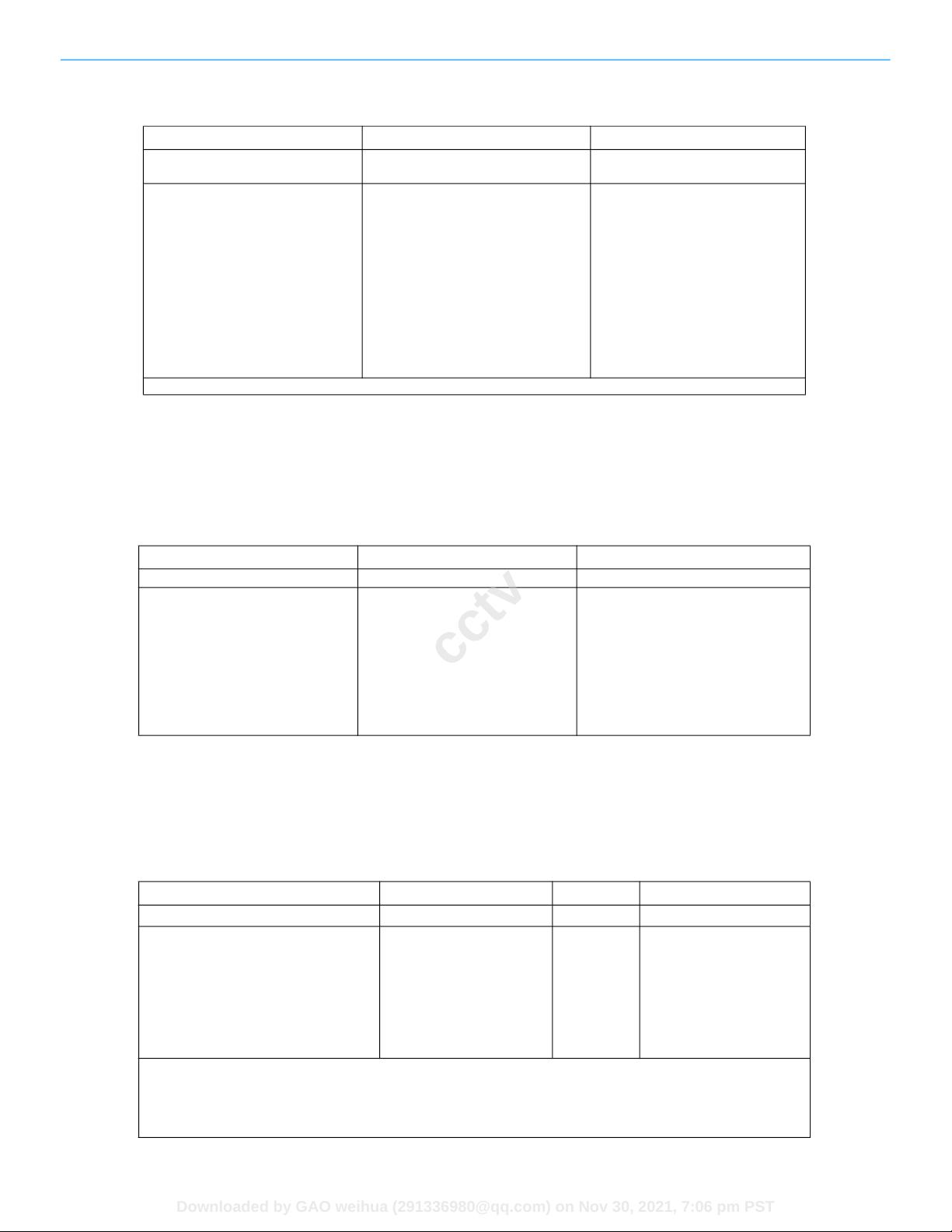
8.1.5 Byte 4 (0x004): SDRAM Density and Banks (Cont’d)
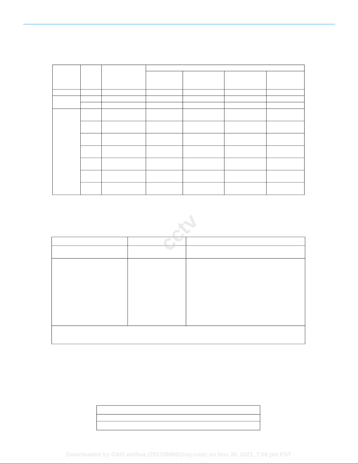
8.1.6 Byte 5 (0x005): SDRAM Addressing
This byte, shown in Table 19, describes the row addressing and the column addressing in the SDRAM device. Bits 2~0 encode the
number of column address bits, and bits 5~3 encode the number of row address bits. These values come from the DDR4 SDRAM
data sheet.
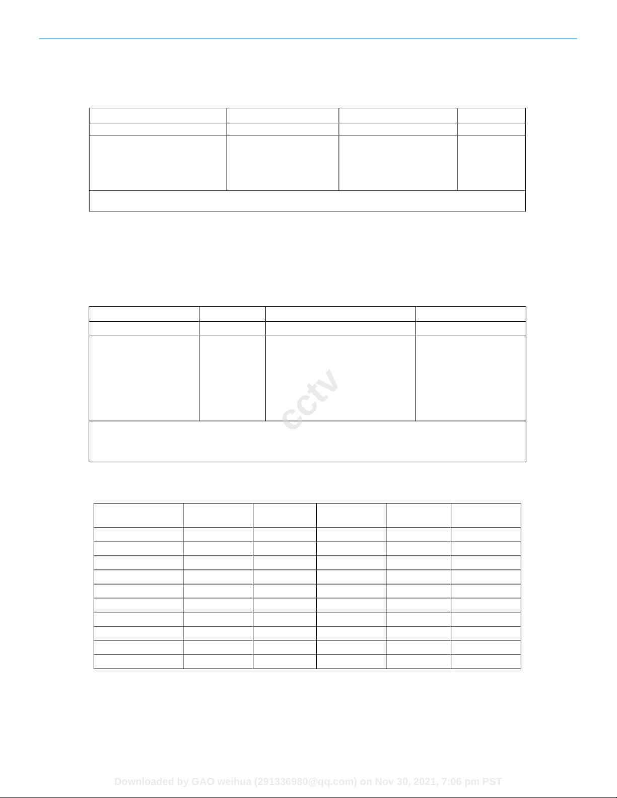
8.1.7 Byte 6 (0x006): Primary SDRAM Package Type
This byte, shown in Table 20, describes the type of SDRAM devices on the module. For modules having asymmetrical assembly of
multiple SDRAM package types, this byte defines the primary set of SDRAMs; Byte 10 defines the secondary set.
Table 18 — Byte 4 (0x004): SDRAM Density and Banks
Bits 7~6 Bits 5~4 Bits 3~0
Bank Group Bits
Bank Address Bits
1
Total SDRAM capacity per die,
in megabits
Bits [7, 6]:
00 = 0 (no bank groups)
01 = 1 (2 bank groups)
10 = 2 (4 bank groups)
11 = reserved
Bit [5, 4] :
00 = 2 (4 banks)
01 = 3 (8 banks)
All others reserved
Bit [3, 2, 1, 0] :
0000 = 256 Mb
0001 = 512 Mb
0010 = 1 Gb
0011 = 2 Gb
0100 = 4 Gb
0101 = 8 Gb
0110 = 16 Gb
0111 = 32 Gb
1000 = 12 Gb
1001 = 24 Gb
All others reserved
NOTE 1 Bank Address Bits determine the number of banks in each Bank Group.
Table 19 — Byte 5 (0x005): SDRAM Addressing
Bits 7~6 Bits 5~3 Bits 2~0
Reserved Row Address Bits Column Address Bits
Reserved; must be coded as 00 Bit [5, 4, 3] :
000 = 12
001 = 13
010 = 14
011 = 15
100 = 16
101 = 17
110 = 18
All others reserved
Bit [2, 1, 0] :
000 = 9
001 = 10
010 = 11
011 = 12
All others reserved
Table 20 — Byte 6 (0x006): Primary SDRAM Package Type
Bit 7 Bits 6~4 Bits 3~2 Bit 1~0
Primary SDRAM Package Type Die Count Reserved
Signal Loading
2
0 = Monolithic DRAM Device
1 = Non-Monolithic Device
1
000 = Single die
001 = 2 die
010 = 3 die
011 = 4 die
100 = 5 die
101 = 6 die
110 = 7 die
111 = 8 die
00
00 = Not specified
3
01 = Multi load stack
10 = Single load stack (3DS)
11 = Reserved
NOTE 1 This includes Dual Die, Quad Die, Multi-Die, 3DS, or physically stacked devices - anything that is outside the
standard monolithic device.
NOTE 2 Refers to loading on signals at the SDRAM balls. Loading on certain signals (CKE, ODT, etc.) per specification
of device stacking as defined in JESD79-4.
NOTE 3 Monolithic DRAM device coded as 00 in bits 1~0.
Downloaded by GAO weihua (291336980@qq.com) on Nov 30, 2021, 7:06 pm PST
cctv
剩余82页未读,继续阅读
2022-07-18 上传
2019-02-12 上传
208 浏览量
2019-08-28 上传
点击了解资源详情
点击了解资源详情

YunQue5908
- 粉丝: 56
- 资源: 26
 我的内容管理
展开
我的内容管理
展开


最新资源
- Elasticsearch核心改进:实现Translog与索引线程分离
- 分享个人Vim与Git配置文件管理经验
- 文本动画新体验:textillate插件功能介绍
- Python图像处理库Pillow 2.5.2版本发布
- DeepClassifier:简化文本分类任务的深度学习库
- Java领域恩舒技术深度解析
- 渲染jquery-mentions的markdown-it-jquery-mention插件
- CompbuildREDUX:探索Minecraft的现实主义纹理包
- Nest框架的入门教程与部署指南
- Slack黑暗主题脚本教程:简易安装指南
- JavaScript开发进阶:探索develop-it-master项目
- SafeStbImageSharp:提升安全性与代码重构的图像处理库
- Python图像处理库Pillow 2.5.0版本发布
- mytest仓库功能测试与HTML实践
- MATLAB与Python对比分析——cw-09-jareod源代码探究
- KeyGenerator工具:自动化部署节点密钥生成
