没有合适的资源?快使用搜索试试~ 我知道了~
首页HMS Anybus-S开发设计指南:DP卡集成与系统详解
HMS Anybus-S开发设计指南:DP卡集成与系统详解
需积分: 9 4 下载量 87 浏览量
更新于2024-07-21
收藏 1.54MB PDF 举报
本篇文档是HMS Industrial Networks公司发布的"Anybus SSlave&Master"系列模块的开发设计指南,标题为"Parallel Interface Design Guide"。该文档主要针对的是Profibus-DP技术,DP卡作为HMS公司的套件产品,旨在为用户深入理解该模块提供的功能提供详尽的指导。 文档首先强调了读者需具备高级软件设计和一般通信系统知识背景,以便更好地理解和应用。重要用户信息部分指出,尽管作者在准备过程中已尽力确保内容的准确性,但读者需了解手册中的数据和示例可能并非最终版,HMS Industrial Networks AB保留根据持续的产品开发策略对产品进行修改的权利。这意味着信息可能会随时间变化,不应视为对HMS工业网络承诺的正式约束。 在文档的核心部分,读者可以期待学习到关于Anybus SSlave和Master模块的接口设计细节,包括但不限于模块的工作原理、协议实现、硬件配置、数据传输特性以及如何与不同的DP设备进行有效连接。此外,可能涉及的内容还包括错误处理、通信性能优化、以及与不同操作系统和编程语言的集成方法。为了充分利用这些功能,开发者需要遵循文档中的指导,以确保系统的可靠性和兼容性。 这是一份技术密集型的参考资料,涵盖了从理论到实践的关键知识点,对于想要在Profibus-DP环境下进行系统设计、编程或维护的工程师来说,是不可或缺的工具。通过阅读并遵循这份文档,用户将能更好地利用Anybus S系列模块,提升其工业自动化解决方案的效率和可靠性。
资源详情
资源推荐
Application Connector 14
Doc.Id. HMSI-27-275
Anybus-S Slave & Master
Doc.Rev. 3.00
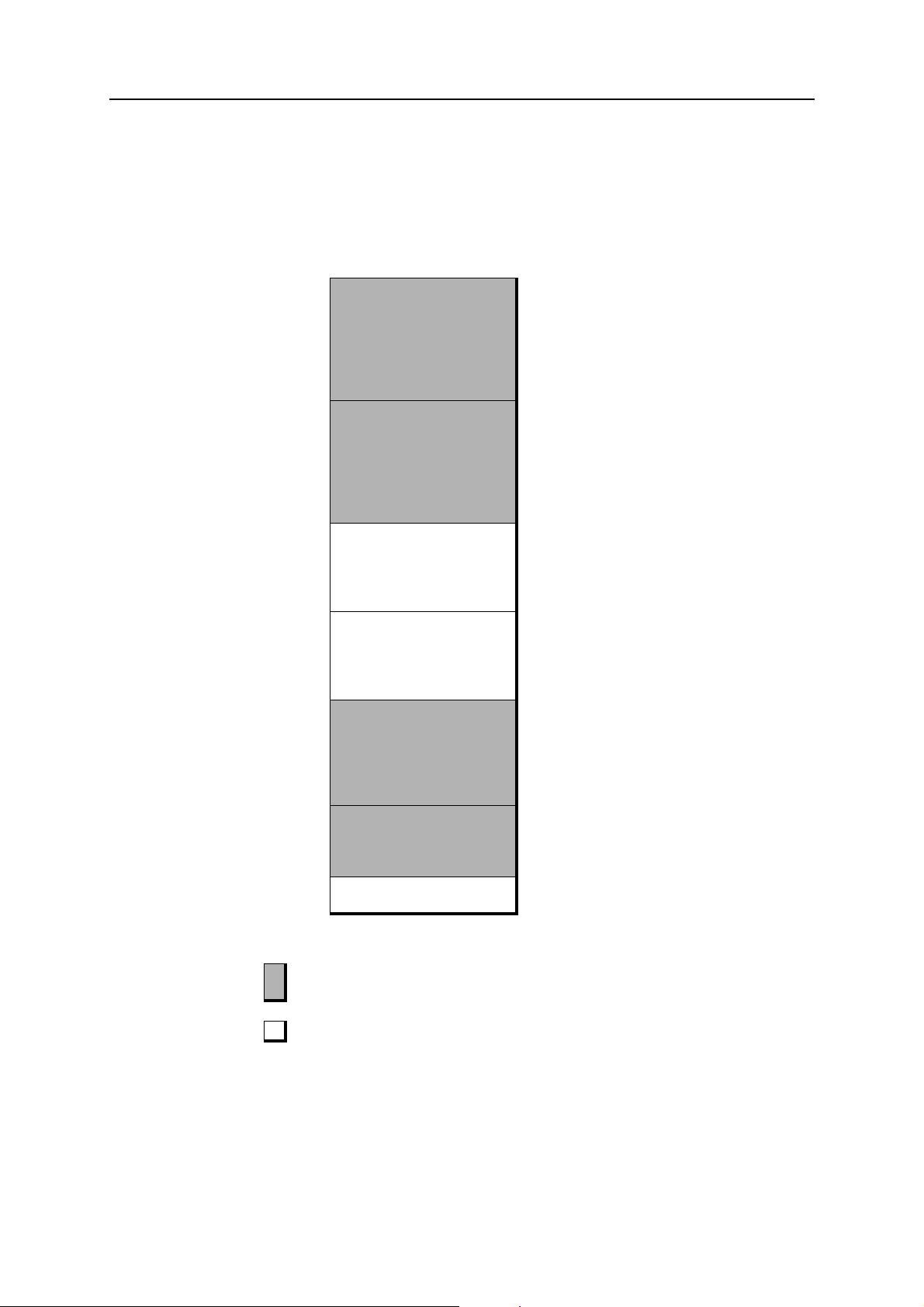
Data Input / Output (D
0
... D
7
)
Data output pins during read operations, or data input pins during write operations. D
0
is the least sig-
nificant bit, D
7
is the most significant.
The target memory location is specified on the Address Inputs (A
0
... A
11
).
Busy Signal (BUSY)
Active low open collector output, internally pulled up with 10k.When low, this pin indicates that the
desired address is currently in use by the Anybus module, and can be used to insert wait states to stall
the current operation until the module is ready.
Interrupt Request (IRQ)
Active low open collector output, internally pulled up with 10k. When low, this pin indicates that new
information is available in the Anybus Indication Register (7FFh). It is strongly recommended to imple-
ment this signal on the host application.
Output Enable (OE)
Enables data output on D
0
... D
7
when low.
Read/Write (R/W)
Enables data input on D
0
... D
7
when low. Internally pulled up with 10k.
Chip Enable (CE)
Active low input (though pulled up on most modules); enables communication with the application in-
terface. CE
must only be active during access of the DPRAM. Internally pulled up with 10k unless
otherwise stated in section ‘Application Interface Hardware Deviances’.
Reset (RESET)
If low, a system reset is initiated.
Internally pulled up with 10k - 75k and decoupled to ground with a 10 - 100nF capacitor.
Application Connector 15
Doc.Id. HMSI-27-275
Anybus-S Slave & Master
Doc.Rev. 3.00
2.3 Asynchronous Serial Interface
These pins are generally used for firmware upgrades etc., see “Firmware Upgrade” on page 65.
For signal characteristics etc., see “Signal Characteristics” on page 79.
Transmit Data (TxD)
Asynchronous serial data transmit signal. Internally pulled up with 10k. Anybus modules with 3,3 to
5V conversion of the Tx signal does not have the 10k resistor. The signal is driven high or low by the
buffer circuit instead. See also “Application Interface Hardware Deviances” on page 75.
Receive Data (RxD)
Asynchronous serial data receive signal. Internally pulled up with 10k.
Doc.Id. HMSI-27-275
Anybus-S Slave & Master
Doc.Rev. 3.00
Chapter 3
3. Memory Map
The dual port memory is subdivided into several smaller areas based on their usage, see memory map
below.
Note: Implementing A11 in the application will affect the memory map. See “Extended Memory Mode
(4K DPRAM)” on page 73 for further information.
Address: Area: Access: Notes:
000h - 1FFh
Input Data Area R/W See “Fieldbus Data Exchange” on page 36
200h - 3FFh Output Data Area RO See “Fieldbus Data Exchange” on page 36
400h - 51Fh Mailbox Input Area R/W See “Mailbox Interface” on page 39
520h - 63Fh Mailbox Output Area RO See “Mailbox Interface” on page 39
640h - 7BFh
Fieldbus Specific Area - (Consult separate fieldbus appendix)
7C0h - 7FDh
Control Register Area R/W See “Control Register Area” on page 17
7FEh - 7FFh
Handshake Registers
R/W
See “Handshaking & Indication Registers” on
page 25
These areas must be allocated before access. See “Handshaking & Indication Registers” on
page 25.
These areas can be accessed directly.
Doc.Id. HMSI-27-275
Anybus-S Slave & Master
Doc.Rev. 3.00
Chapter 4
4. Control Register Area
This area contains information about the Anybus module; revision, initialization parameters, fieldbus
type and status etc. This area also contains registers for Watchdog handling and Event Notification han-
dling.
Note: Generally, the Control Register Area must be allocated by the application before access. Howev-
er, during module initialization, it is allowed to read static data such as software revision, fieldbus type,
module type etc. without handshaking.
Address: Register: Access: Notes:
7C0h - 7C1h Bootloader Version RO
7C2h - 7C3h
Application Interface Software Version
a
a. On modules with application interface versions prior to 2.00, this register is reserved and should be zero.
RO
7C4h - 7C5h
Fieldbus software version
a
RO
7C6h - 7C9h Module Serial Number RO Unique serial number
7CAh - 7CBh Vendor ID RO Manufacturer ID number (HMS, other)
7CCh - 7CDh Fieldbus Type RO Fieldbus type identifier
7CEh - 7CFh Module Software Version RO Software revision
7D0h - 7D1h
(reserved) -
7D2h - 7D3h Watchdog Counter Input R/W Application controlled Watchdog counter
7D4h - 7D5h Watchdog Counter Output RO Counter, incremented each 1ms
7D6h - 7D9h
(reserved) -
7DAh - 7DDh LED Status RO Current status of each fieldbus status indicator
7DEh - 7DFh
(reserved) -
7E0h - 7E1h Module Type RO Module type, master, slave, other.
7E2h - 7E3h Module Status RO Bit information; freeze, clear etc.
7E4h - 7EBh Changed Data Field RO Bit field, indicating changes in the Output Data
Area in the Dual Port Memory
7ECh - 7EDh Event Notification Cause R/W Event cause register
7EEh - 7EFh Event Notification Source RO Configuration register for Event Notification
7F0h - 7F1h Input I/O Length RO Input I/O size
7F2h - 7F3h Input DPRAM Length RO Number of input I/O bytes in dual port memory
7F4h - 7F5h Input Total Length RO Total Input Data size
7F6h - 7F7h Output I/O Length RO Output I/O size
7F8h - 7F9h Output DPRAM Length RO Number of output I/O bytes in dual port memory
7FAh - 7FBh Output Total Length RO Total Output Data size
7FCh - 7FDh
(reserved) -
剩余81页未读,继续阅读
marbury
- 粉丝: 0
- 资源: 4
上传资源 快速赚钱
- 我的内容管理 展开
- 我的资源 快来上传第一个资源
- 我的收益 登录查看自己的收益
- 我的积分 登录查看自己的积分
- 我的C币 登录后查看C币余额
- 我的收藏
- 我的下载
- 下载帮助
最新资源
- OptiX传输试题与SDH基础知识
- C++Builder函数详解与应用
- Linux shell (bash) 文件与字符串比较运算符详解
- Adam Gawne-Cain解读英文版WKT格式与常见投影标准
- dos命令详解:基础操作与网络测试必备
- Windows 蓝屏代码解析与处理指南
- PSoC CY8C24533在电动自行车控制器设计中的应用
- PHP整合FCKeditor网页编辑器教程
- Java Swing计算器源码示例:初学者入门教程
- Eclipse平台上的可视化开发:使用VEP与SWT
- 软件工程CASE工具实践指南
- AIX LVM详解:网络存储架构与管理
- 递归算法解析:文件系统、XML与树图
- 使用Struts2与MySQL构建Web登录验证教程
- PHP5 CLI模式:用PHP编写Shell脚本教程
- MyBatis与Spring完美整合:1.0.0-RC3详解
资源上传下载、课程学习等过程中有任何疑问或建议,欢迎提出宝贵意见哦~我们会及时处理!
点击此处反馈
安全验证
文档复制为VIP权益,开通VIP直接复制
信息提交成功