AD8630ARZ-REEL7 芯片中文规格说明书:高性能运算放大器
需积分: 5 94 浏览量
更新于2024-06-25
收藏 1.36MB PDF 举报
"AD8630ARZ-REEL7是ADI公司的一款电子元器件,具体来说是一款零漂移、单电源、轨至轨输入/输出运算放大器的规格手册。这款运算放大器适用于多种应用,特别是在汽车传感器、压力和位置传感器、应变仪放大器以及医疗仪器等领域有广泛应用。"
AD8630ARZ-REEL7的主要特点包括:
1. **最低的自动零噪声**:这款运算放大器具备极低的自动零噪声性能,确保了在信号处理时的高精度和低噪声干扰。
2. **超低偏置电压**:其输入偏置电压仅为1微伏(1µV),这意味着在工作过程中,电路的初始误差极小,提高了系统的准确度。
3. **输入偏置电流极低**:最大输入偏置电流仅为100皮安(100pA),这使得AD8630在需要低偏置电流的敏感应用中表现出色。
4. **轨至轨输入和输出摆动**:AD8630可以在电源电压范围内实现输入和输出的全范围操作,增加了设计的灵活性。
5. **5V单电源操作**:适合在低电压供电环境中使用,简化了电源管理。
6. **高增益、共模抑制比(CMRR)和电源抑制比(PSRR)**:达到130分贝,保证了在不同电源条件和信号源共模电压下仍能保持良好的性能。
7. **快速过载恢复时间**:过载恢复时间仅为50微秒,表明其在瞬态过载情况下的响应速度非常快。
8. **无需外部组件**:简化了电路设计,降低了系统成本。
9. **适用于汽车应用**:经过资格认证,满足汽车电子设备的严格标准。
这些特性使得AD8630ARZ-REEL7成为需要高精度、低噪声、低功耗和宽输入输出范围的电子系统设计的理想选择。在汽车工业中,例如在汽车传感器(如温度、压力或速度传感器)、位置检测和应变仪放大器中,它的性能可以显著提高测量的准确性和稳定性。在医疗仪器领域,其低噪声和高精度特性对于生理信号的检测和分析也至关重要。
值得注意的是,尽管ADI公司提供的信息被认为是准确和可靠的,但使用该芯片时仍需用户自行承担风险,并且没有对第三方专利或权利的侵犯提供任何明示或暗示的许可。此外,规格可能会随时间变化而不事先通知,因此在设计时应关注最新的数据手册。最后,所有的商标和注册商标均归各自所有者所有。
Data Sheet AD8628/AD8629/AD8630
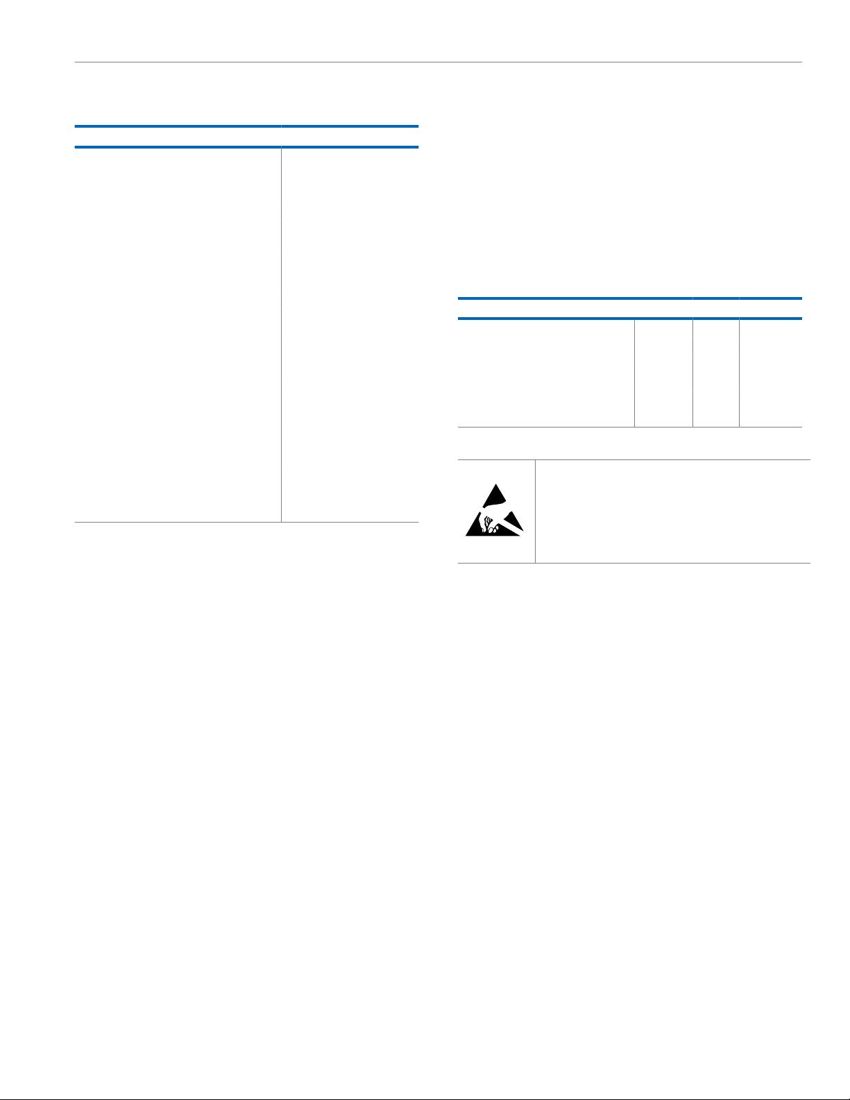
ABSOLUTE MAXIMUM RATINGS
analog.com Rev. M | 5 of 21
Table 3.
Parameter Rating
Supply Voltage 6 V
Input Voltage GND – 0.3 V to V
S
+ 0.3 V
Differential Input Voltage
1
±5.0 V
Output Short-Circuit Duration to GND Indefinite
Storage Temperature Range −65°C to +150°C
Operating Temperature Range −40°C to +125°C
Junction Temperature Range −65°C to +150°C
Lead Temperature (Soldering, 60 sec) 300°C
ESD AD8628
HBM 8-Lead SOIC ±7000V
FICDM 8-Lead SOIC ±1500V
FICDM 5-Lead TSOT ±1000V
MM 8-Lead SOIC ±200V
ESD AD8629
HBM 8-Lead SOIC ±4000V
FICDM 8-Lead SOIC ±1000V
ESD AD8630
HBM 14-Lead SOIC ±5000V
FICDM 14-Lead SOIC ±1500V
FICDM 14-Lead TSSOP ±1500V
MM 14-Lead SOIC ±200V
1
Differential input voltage is limited to ±5 V or the supply voltage, whichever is
less.
Stresses at or above those listed under Absolute Maximum Ratings
may cause permanent damage to the product. This is a stress
rating only; functional operation of the product at these or any other
conditions above those indicated in the operational section of this
specification is not implied. Operation beyond the maximum operat-
ing conditions for extended periods may affect product reliability.
THERMAL CHARACTERISTICS
θ
JA
is specified for worst-case conditions, that is, θ
JA
is specified for
the device soldered in a circuit board for surface-mount packages.
This was measured using a standard two-layer board.
Table 4.
Package Type θ
JA
θ
JC
Unit
5-Lead TSOT (UJ-5) 207 61 °C/W
5-Lead SOT-23 (RJ-5) 230 146 °C/W
8-Lead SOIC_N (R-8) 158 43 °C/W
8-Lead MSOP (RM-8) 190 44 °C/W
14-Lead SOIC_N (R-14) 105 43 °C/W
14-Lead TSSOP (RU-14) 148 23 °C/W
ESD CAUTION
ESD (electrostatic discharge) sensitive device. Charged devi-
ces and circuit boards can discharge without detection. Although
this product features patented or proprietary protection circuitry,
damage may occur on devices subjected to high energy ESD.
Therefore, proper ESD precautions should be taken to avoid
performance degradation or loss of functionality.
剩余21页未读,继续阅读
点击了解资源详情
点击了解资源详情
点击了解资源详情
2023-05-30 上传
2023-05-30 上传
点击了解资源详情
2023-05-30 上传
2023-05-30 上传
2023-05-31 上传

芯脉芯城
- 粉丝: 4
- 资源: 4030
 我的内容管理
展开
我的内容管理
展开


最新资源
- netgamemud.rar_Delphi_
- hakuen
- RxSwift实现ComposableArchitecture-Swift开发
- Crewmate:“我们之间”交叉兼容服务器,用于自定义游戏模式和改装!
- log4j2-json-layout:Log4J 2 JSON布局插件
- fromedi:EDI到人类语言的翻译器
- OSEK完整版源码.rar
- DS1302.zip
- PyQt:PyQt示例(PyQt各种测试和例子)PyQt4 PyQt5
- Emoji Keyboard-crx插件
- clockwork-rnn-in-pytorch:该存储库包含使用pytorch的发条rnn的实现
- 高仿某讯网平台登录页
- 适用于iOS的完全可自定义的水平圆选择器视图-Swift开发
- 客户关系管理
- LCD1602_4X4key.rar_单片机开发_C/C++_
- This-Repo-Has-1635-Stars:对,是真的
