Functional Description
DS312-2 (v1.1) March 21, 2005 www.xilinx.com 11
Advance Product Specification
R
I/O Banking Rules
When assigning I/Os to banks, these V
CCO
rules must be
followed:
1. All V
CCO
pins on the FPGA must be connected even if a
bank is unused.
2. All V
CCO
lines associated within a bank must be set to
the same voltage level.
3. The V
CCO
levels used by all standards assigned to the
I/Os of any given bank must agree. The Xilinx
development software checks for this. Table 3 and
Table 4 describe how different standards use the V
CCO
supply.
4. If a bank does not have any V
CCO
requirements,
connect V
CCO
to an available voltage, such as 2.5V or
3.3V. Some configuration modes might place additional
V
CCO
requirements. Refer to Configuration, page 56
for more information.
If any of the standards assigned to the Inputs of the bank
use V
REF
, then the following additional rules must be
observed:
1. All V
REF
pins must be connected within a bank.
2. All V
REF
lines associated with the bank must be set to
the same voltage level.
3. The V
REF
levels used by all standards assigned to the
Inputs of the bank must agree. The Xilinx development
software checks for this. Table 3 describes how different
standards use the V
REF
supply.
If V
REF
is not required to bias the input switching thresholds,
all associated V
REF
pins within the bank can be used as
user I/Os or input pins.
Package Footprint Compatibility
Sometimes, applications outgrow the logic capacity of a
specific Spartan-3E FPGA. Fortunately, the Spartan-3E
family is designed so that multiple part types are available in
pin-compatible package footprints, as described in Module
4. In some cases, there are subtle differences between
devices available in the same footprint. These differences
are outlined for each package, such as pins that are uncon-
nected on one device but connected on another in the same
package or pins that are dedicated inputs on one package
but full I/O on another. When designing the printed circuit
board (PCB), plan for potential future upgrades and pack-
age migration.
The Spartan-3E family is not pin-compatible with any previ-
ous Xilinx FPGA family.
Dedicated Inputs
Dedicated Inputs are IOBs used only as inputs. Pin names
designate a Dedicated Input if the name starts with
IP
, for
example, IP or IP_Lxxx_x. Dedicated inputs retain the full
functionality of the IOB for input functions with a single
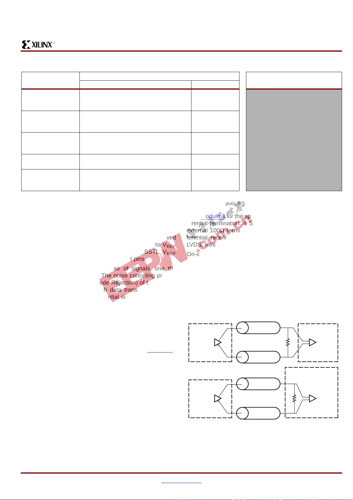
exception for differential inputs (IP_Lxxx_x). For the differ-
ential Dedicated Inputs, the on-chip differential termination
is not available. To replace the on-chip differential termina-
tion, choose a differential pair that supports outputs
(IO_Lxxx_x) or use an external 100Ω termination resistor on
the board.
ESD Protection
Clamp diodes protect all device pads against damage from
Electro-Static Discharge (ESD) as well as excessive voltage
transients. Each I/O has two clamp diodes: one diode
extends P-to-N from the pad to V
CCO
and a second diode
extends N-to-P from the pad to GND. During operation,
these diodes are normally biased in the off state. These
clamp diodes are always connected to the pad, regardless
of the signal standard selected. The presence of diodes lim-
its the ability of Spartan-3E I/Os to tolerate high signal volt-
ages. The V
IN
absolute maximum rating in Table 1 of
Module 3
specifies the voltage range that I/Os can tolerate.
Supply Voltages for the IOBs
The IOBs are powered by three supplies:
1. The V
CCO
supplies, one for each of the FPGA’s I/O
banks, power the output drivers. The voltage on the
V
CCO
pins determines the voltage swing of the output
signal.
2. V
CCINT
is the main power supply for the FPGA’s internal
logic.
3. V
CCAUX
is an auxiliary source of power, primarily to
optimize the performance of various FPGA functions
such as I/O switching.
The I/Os During Power-On, Configuration, and
User Mode
All I/Os have ESD clamp diodes to their respective V
CCO
supply and from GND, as shown in Figure 1. The V
CCINT
(1.2V), V
CCAUX
(2.5V), and V
CCO
supplies can be applied in
any order. Before the FPGA can start its configuration pro-
cess, V
CCINT
, V
CCO
Bank 2, and V
CCAUX
must have
reached their respective minimum recommended operating
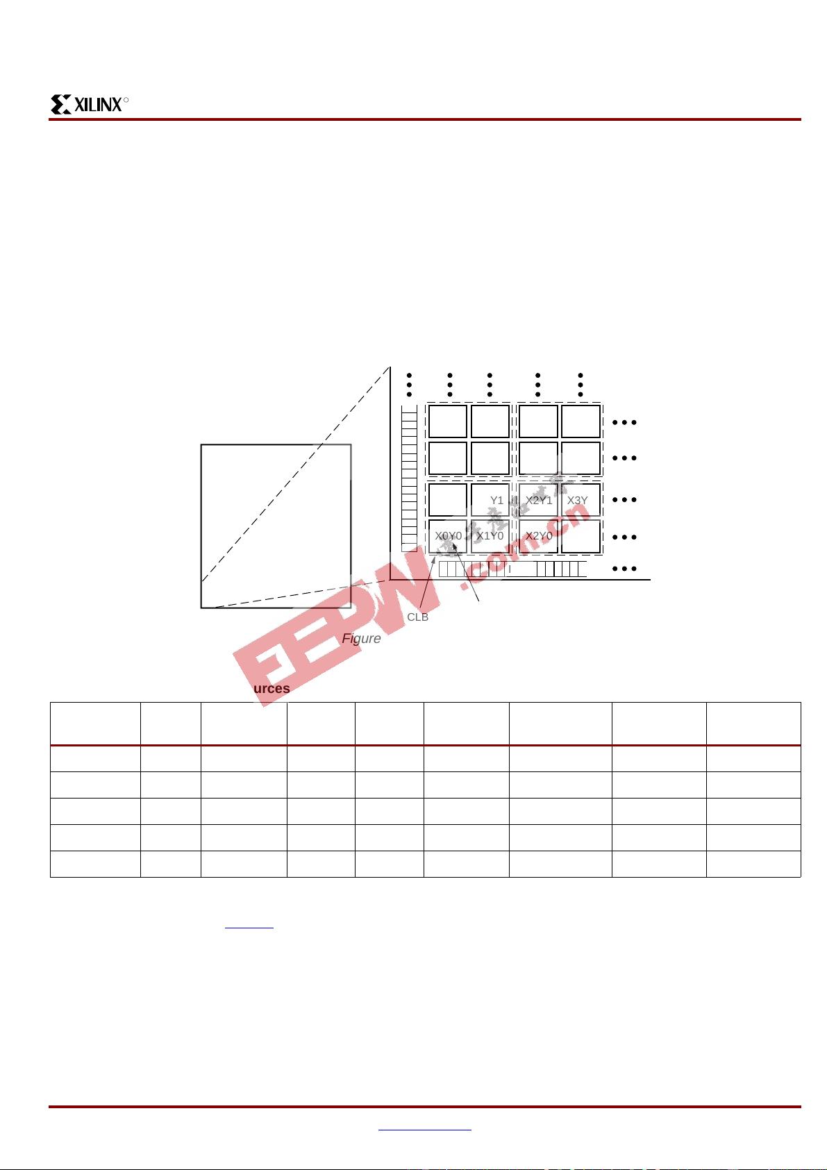
Figure 10:
Spartan-3E I/O Banks (top view)
DS312-2_26_021205
Bank 0
Bank 2
Bank 3
Bank 1


