100 Gbit/s Scrambler Architectures for OTN Protocol:
FPGA Implementation and Result Comparison
Arley Salvador, Valentino Corso
CPqD Research and Development Center in Telecommunications
Campinas, Brazil
arleys@cpqd.com.br
Abstract— This paper describes and compares two scrambler
architectures developed and implemented in an advanced field
programmable gate array (FPGA), with applications in
100 Gbit/s optical transport network (OTN) systems.
I. INTRODUCTION
Due to the increasing utilization of channel bandwidth
combined with the necessity to concentrate and control data
in optical communication transmission systems, resulted on a
standardized transmission protocol by ITU-T (International
Telecommunication Union) G.709 [1]. This recommendation
defines the network interfaces for optical fiber links up to 100
Gbit/s. In these optical transport network (OTN) systems,
clock signals are recovered from the incoming data stream
and, long sequences of consecutive digits (zeros or ones) are
avoided through the use of digital scrambling techniques. Due
to the complexity of OTN equipment devices, designers avoid
the over-consumption of logic resources. This paper presents
a comparison between two different low gate count scrambler
architectures and indicates the most suitable solution.
Section II briefly describes the OTN scrambler, according
to the recommendation specifications. Section III and IV
present scrambler architectures implemented with
combinational logic (logical scrambler) and registers
(registered scrambler), respectively. The comparison of these
two architectures is presented in section V. Finally,
conclusions are shown in section VI.
II. OTN
SCRAMBLER
A scrambler module performs data scrambling by
implementing an exclusive-OR operation between two data
streams: the transmitted information and the pseudorandom
bit sequence (PRBS) generator.
The OTN scrambler is described by ITU-T G.709
recommendation [1] and uses the polynomial x
16
+ x
12
+ x
3
+
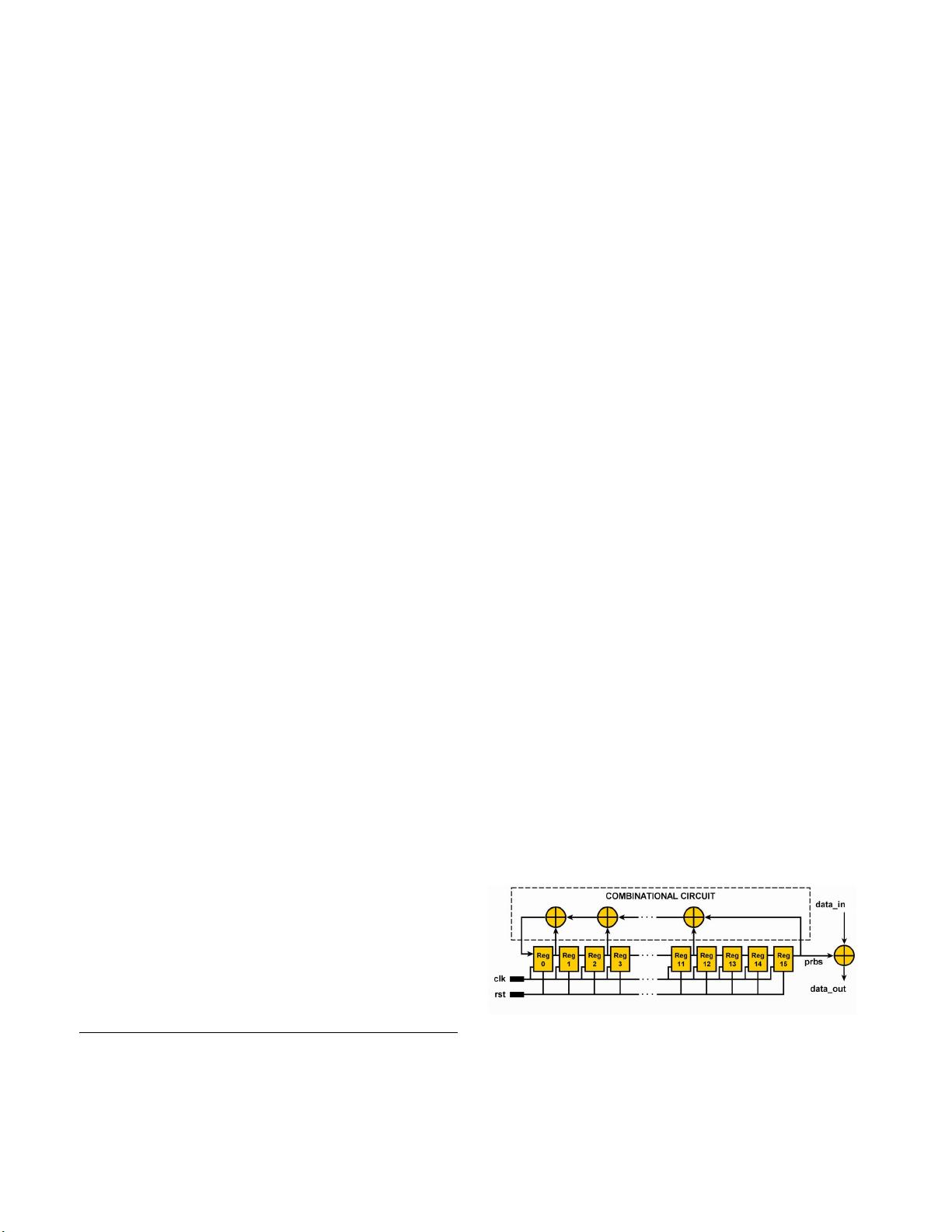
x + 1. The G.709 scrambler circuit with a serial PRBS
generator is shown in Fig. 1 [5]. However, this architecture
has to be adapted depending on the transmission frequency or
on the data rate, since very high speed serial processing is not
feasible with the current technology [4].
The scramblers that will be presented in the next sections
can be implemented using an FPGA that can operate with
data rates up to 100 Gbit/s, using parallel buses of 640 bits
which will processes the data on each clock cycle at an
internal frequency of 156.25 MHz.
Whenever a FAS (Frame Alignment Signal) word is
received in the OTN data stream, the scrambler is initialized
by setting all the registers. When it happens, the circuit starts
scrambling all the data immediately after this FAS field until
the reception of the next FAS, in the following OTN frame
[1][6].
The scrambler circuit architectures which will be
compared in this document have their PRBS circuits
implemented in two different ways.
Each circuit, from now on, will be treated as a “logical
scrambler” and “registered scrambler”. These both cases are
described in the following sections.
III. L
OGICAL SCRAMBLER
Fig. 2 depicts a general block diagram of a logical
scrambler. The architecture of this module implements a
register set which are feedback through a combinational
circuit [2][3].
The pseudorandom signal generated by the circuit feed
the output bus called prbs[(L-1)..0], where L represents the
number of output bits.
This research was supported by Funttel – Fundo para o Desenvolvimento
Tecnológico das Telecomunicações.
Fig. 1. G.709 Serial scrambler block diagram [1].


