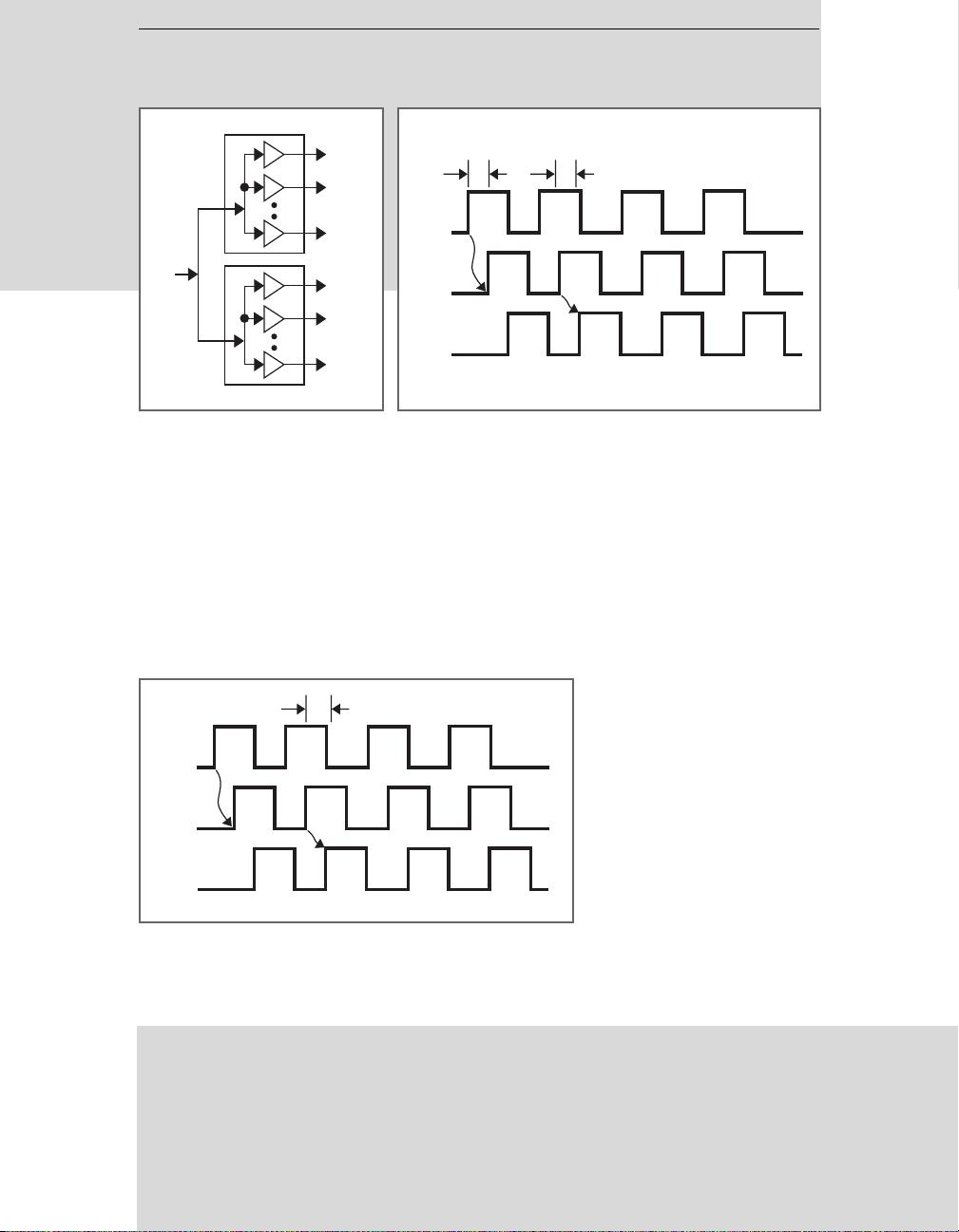
The 10 ns t
PD
clock driver delay shown in Figure 2.5 does not take into account the affects
of the board layout and design. These types of devices are excellent for buffering source
signals such as oscillators where the output phase does not need to match the input. A
variety of the non-PLL based buffers are available on the market today and typically range
from as few as 4 outputs to as many as 30. Some devices also include configurable I/O and
internal registers to divide the output frequencies.
Among the highest performance non-PLL based Low Voltage CMOS (LVCMOS) clock buffers
available today is the B9940L. The B9940L is a low-voltage clock distribution buffer with
the capability to select either a differential LVPECL or a LVCMOS/LVTTL compatible input
clock. The two clock sources can be used to provide for a test clock as well as the primary
system clock. All other control inputs are LVCMOS/LVTTL-compatible. The eighteen
outputs are 2.5V- or 3.3V-compatible and can drive two series terminated 50-Ohm
transmission lines. With this capability, the B9940L has an effective fanout of 1:36. Low
output-to-output skews of 150 ps, a device to device skew of 750 ps, and a high-end
operating frequency of 200 MHz, makes the B9940L an ideal clock distribution buffer for
nested clock trees in synchronous systems.
These devices still face the problems of device propagation delay. The propagation delay
through these devices is about 5 ns. This delay will cause skew in systems where both the
reference clock to the buffer and the outputs of the buffer need to be aligned. These
devices also have the drawback that the output waveform is directly based on the input
waveform. If the input waveform is a non-50% duty-cycle clock, the output waveform will
also have a less-than-ideal duty cycle. Expensive crystal oscillators with tight tolerances are
needed when using this type of buffer in systems requiring near 50/50 outputs.
These devices also lack the ability to phase adjust or frequency multiply their outputs. Phase
adjustment allows the clock driver to compensate for trace propagation delay mismatches
and setup and hold time differences, and frequency multiplication allows the distribution
of high and low frequency clocks from the same common reference. Expensive
components and time-consuming board routing techniques must be used to compensate
for the functional shortcomings of these buffer-style clock driver devices. PLL-based devices
have been incorporated to address all of these shortcomings.
PLL-Based Clock Drivers
The second type of clock distribution device uses a feedback input that is a function of one
of its outputs. The feedback input can be connected internally or externally to the part. If
it’s an external feedback, a trace is used to connect an output pin to the feedback pin. This
type of device is usually based upon one or more PLLs that are used to align the phase and
frequency of the feedback input and the reference input. Since the feedback input is a
reflecion of an output pin, the propagation delay is effectively eliminated. In addition to
very low device propagation delay, this type of architecture enables output signals to be
phase shifted to compensate for board-level trace-length mismatches. Outputs can be
selectively divided, multiplied, or inverted while still maintaining very low output skew.
2-7
CLOCK BUFFER BASICS CHAPTER
2


