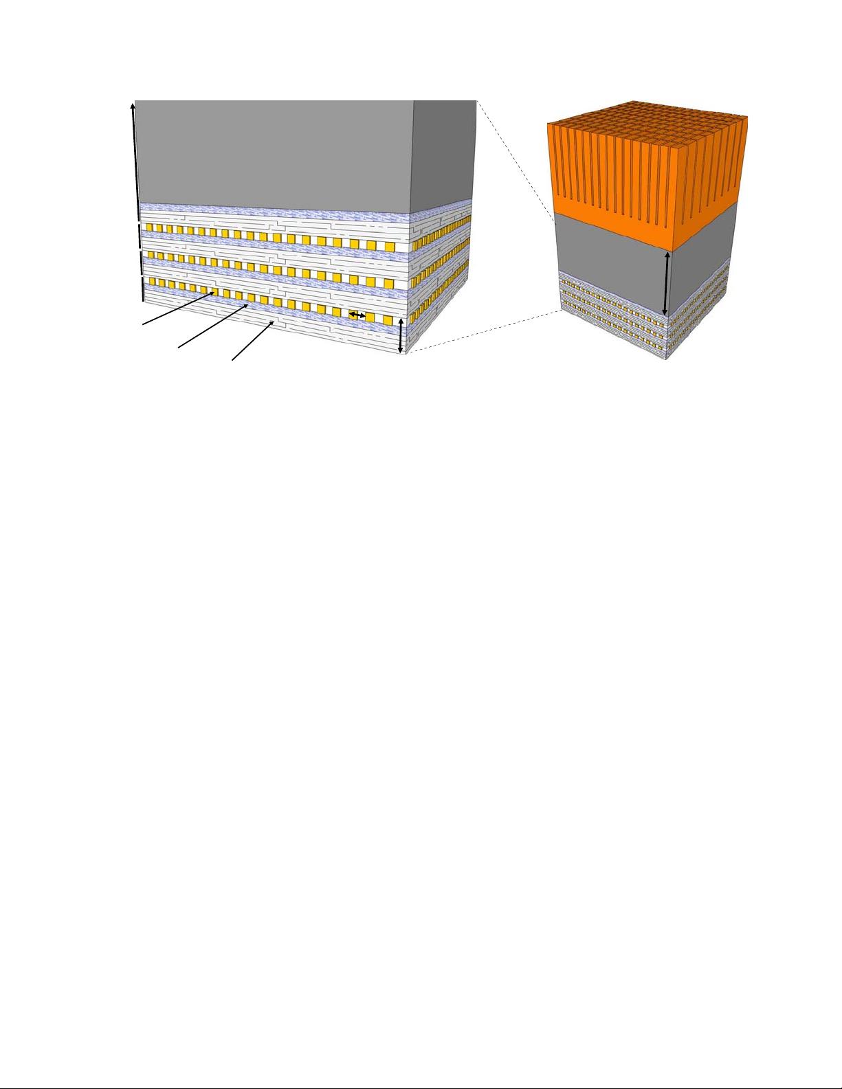
Layer 1
Layer 2
Layer 3
Layer 4
Through Silicon
Vias (TSVs)
Metal Layers
Transistors
10−50um
800−1000um
Bulk Silicon
Heat Sink
< 10um
Figure 2. Cross-sectional view of 3D-stacked dies with a face-to-back topology (not drawn to scale).
typical metal routes, they are very short since each wafer
is thinned to only tens of microns. The TSVs have been
reported to have pitches of only 4-10μm [14]. Even at the
high-end with a 10μm TSV-pitch, a 1024-bit bus would only
require an area of 0.32mm
2
. To put that in perspective, a
1cm
2
chip could support over three hundred of these 1Kb
buses. For the purposes of stacking DRAM, the TSV size
and latency will likely not be a limiting factor for several
generations.
2.3. 3D-Stacked DRAM
Previous studies have already started exploring the perfor-
mance benefits of using 3D integration to stack main mem-
ory on top of a processor. Figure 3(a) shows a tradi-
tional 2D processor core with multiple layers of 3D-stacked
DRAM [20, 24, 26]. The 3D TSVs implement a vertical bus
across the layers to connect the DRAM layers to the proces-
sor core. Independent of the required latencies, the topol-
ogy and overall architecture of these processor-memory 3D
organizations are no different than that used in traditional
off-chip memories. Liu et al. [24] and Kgil et al. [20] do
consider using the dense TSV interface to implement wider
buses, which are traditionally limited by pin-count, but they
do not observe a large performance benefit due to the small
sizes of their workloads and critical-word-first delivery of
data from memory.
The previous approaches do not fully exploit 3D stack-
ing technology because the individual structures are all still
inherently two-dimensional. Tezzaron Corporation has an-
nounced “true” 3D DRAMs where the individual bitcell ar-
rays are stacked in a 3D fashion [38, 39]. Figure 3(b) shows
the overall organization. The top N layers consist of the
stacked DRAM bitcells; this stacked organization reduces
the lengths of internal buses, wordlines and bitlines, which
in turn reduces the access latency of the memory. The bot-
tom layer implements the various control and access circuits,
such as the row decoder, sense amplifiers, row buffers and
output drivers. The advantage of isolating the peripheral
circuitry to a separate, dedicated layer is that different pro-
cess technologies can be incorporated. The DRAM bitcells
are all implemented in a traditional NMOS technology opti-
mized for density, whereas the peripheral circuits are imple-
mented on a CMOS layer optimized for speed. The combi-
nation of reducing bitline capacitance and using high-speed
logic provides a 32% improvement in memory access time
(t
RAS
) for a five-layer DRAM (four layers of memory plus
one layer of logic). Note that this latency reduction is for
the memory array access itself, and this is additive with any
benefits due to placing the memory closer to the processor.
2.4. Methodology and Assumptions
In this section, we briefly describe the processor microar-
chitecture, memory system and 3D integration assumptions
that we use. We base our baseline processor on the Intel
45nm “Penryn” model [19], detailed in Table 1, extended
to a quad-core configuration. We use the SimpleScalar
toolset for the x86 ISA for performance evaluation [3], and
we extended it to perform cycle-level modeling of a multi-
core processor. The simulator models the contention for
cache/memory buses, MSHR capacity, traffic due to write-
back and prefetches, and memory controller request queue
capacity. For the DRAM, we model the low-level tim-
ing including precharge delays (including when it can be
overlapped with other commands), different timings for row
buffer hits and misses, and the effects of periodic DRAM
refreshing. We assume a memory controller implementation
that attempts to schedule accesses to the same row together
to increase row buffer hit rates [34]. For the off-chip DRAM,
we assume a refresh period of 64ms, and the on-chip ver-
455455


