492 Memory Systems: Cache, DRAM, Disk
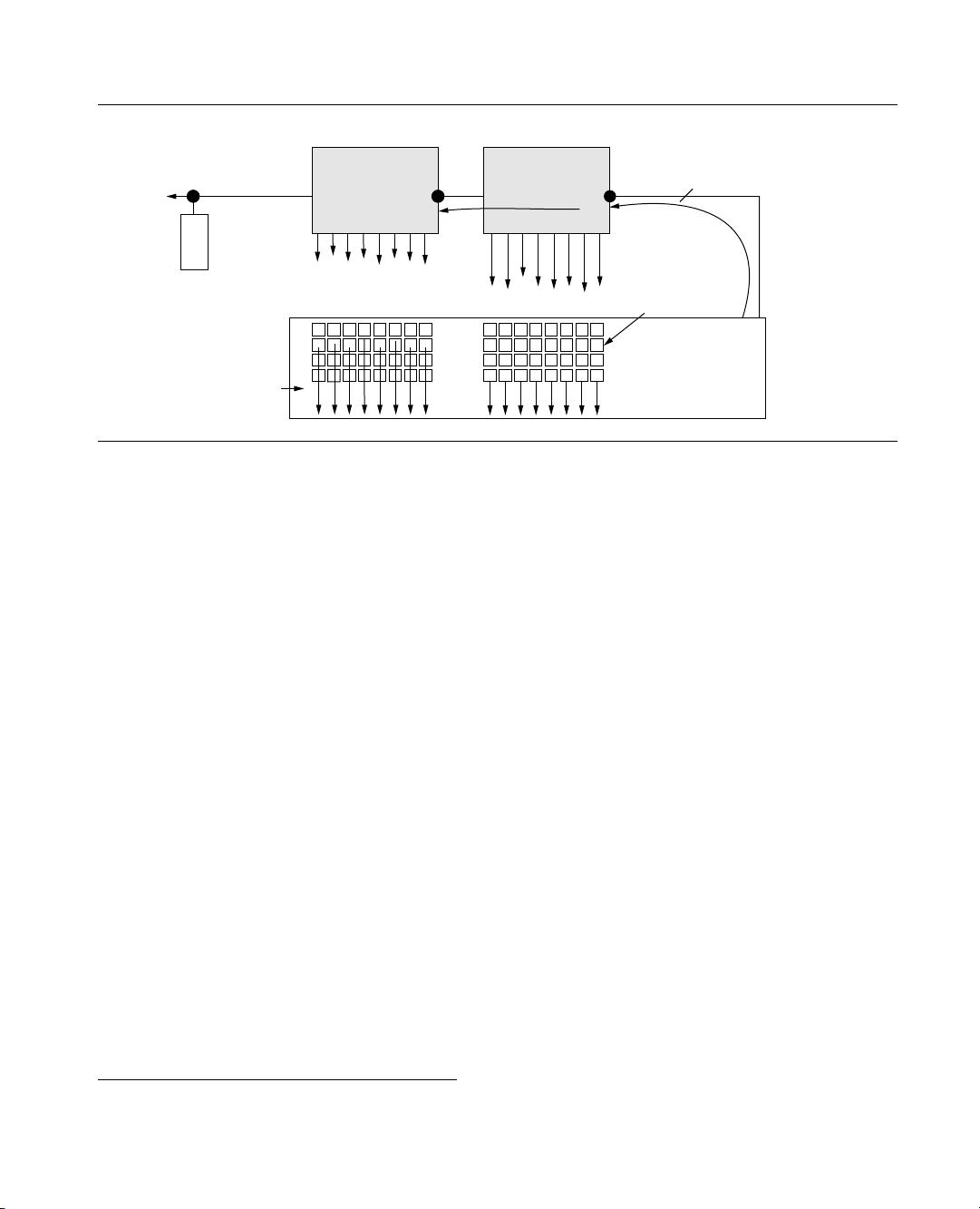
that in the XDR memory system, as in DDRx SDRAM
systems, the command-and-address busses operates
at a relatively lower data rate as compared to the data
bus. In the XDR memory system, the command and
address datapath is a path-length-matched, unidirec-
tional datapath that the XDR memory controller uses
to broadcast command and address information to
DRAM devices. Figure 12.33 also shows that the XDR
controller uses FlexPhase to do skew compensation
on the datapath—removes skew on read data coming
into the controller and adds skew to ensure that write
data reaches DRAM device interface in sync.
Device Architecture
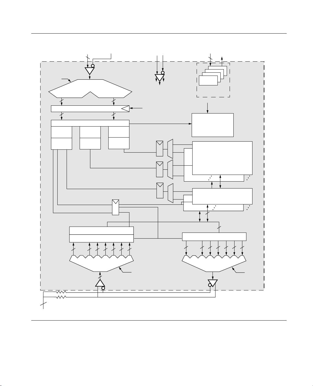
Figure 12.34 illustrates the device organization
of an XDR device. The XDR DRAM device is char-
acterized by numerous features that distinguish it
from the Direct RDRAM device. For example, the
XDR DRAM device has a prefetch length of 16, so
the minimum burst length is 16. However, the XDR
device architecture has been designed with vari-
able device data bus width control so that a device
may be confi gured with a data bus width as low as 1
bit. Consequently, the minimum granularity of data
movement in such a device may be as small as 16
bits. Figure 12.34 also shows that the XDR device
is internally organized into two different, odd and
even, bank sets.
Finally, Figure 12.34 shows that the XDR device
differs from the Direct RDRAM device in that unlike
the Direct RDRAM device, the XDR DRAM device has
a common command bus that is used by row access
commands as well as column access commands.
Moreover, unlike the Direct RDRAM device, the XDR
DRAM device does not have a write buffer. Instead,
it relies on the differing bank sets and an intelligent
controller to alleviate the write-to-read data bus
turnaround issue.
Signaling
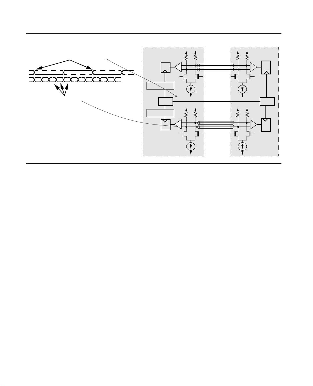
Figure 12.35 shows the octal data rate signaling
system that Rambus Corp. introduced with the XDR
memory system. In this signaling system, a relatively
slow master clock signal (400~800 MHz) is shared by
both the memory controller and the DRAM device. The
DRAM device and the memory controller use current
mirrors to transmit differential signals that are locked
in-phase with the system clock signal, but operate at
four times the frequency of the system clock signal.
Data is transmitted on both edges of the signal, so 8
1-bit symbols per pin pair are transmitted in every
clock cycle. The low voltage swing, point-to-point,
differential signaling enables high bandwidth in com-
modity ASIC and DRAM processor technologies at the
cost of higher power consumption.
FlexPhase
In the XDR memory system, Rambus Corp. uses
a system of bit-adjustable DLL circuitry to remove
bit-to-bit signal skew from the high-speed parallel
data bus. This system of bit-adjustable DLL circuitry
is referred to as FlexPhase. Figure 12.35 shows how
Rambus uses the FlexPhase circuit to account for dif-
ferences in signal fl ight time. FlexPhase takes care
of data-to-data skew, and it can be recalibrated to
lock in new phase differentials to account for ther-
mal drifts between cold and warm systems. Figure
12.35 shows that the FlexPhase circuitry is placed
in the controller interface. In this manner, the Flex-
Phase technology removes the path-length matching
requirement from the XDR memory system without
increasing the cost of the DRAM device. In this case,
the additional cost is paid for in terms of increased
controller sophistication.
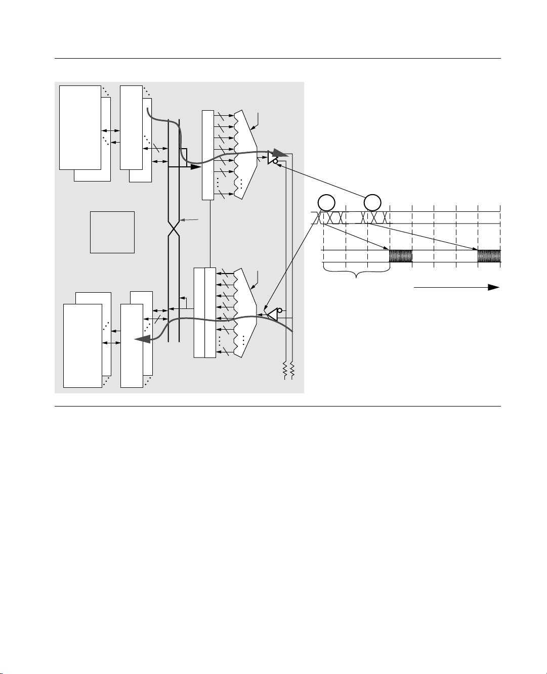
XDR Early Read After Write
To counter the various drawbacks of a write buffer
in Direct RDRAM devices, Rambus did not include
write buffers in the design of its next-generation,
high-performance XDR DRAM device. Instead, XDR
DRAM devices are architected to support a feature
that Rambus refers to as the Early Read After Write
(ERAW) feature. Essentially, XDR devices avoid the
large write-to-read command overhead by using sepa-
rate internal paths for banks separated into odd and
even sets. In this organization, a read command can
proceed in parallel with a write command, as long as
the read and write commands are directed to banks in


