
AD7740
REV. C
–3–
(VDD = 3.0 V to 3.6 V, 4.75 V to 5.25 V, GND = O V, REFIN = 2.5 V)
Limit at T
MIN
, T
MAX
Limit at T
MIN
, T
MAX
Parameter VDD = 3.0 V to 3.6 V VDD = 4.75 V to 5.25 V Unit Conditions/Comments
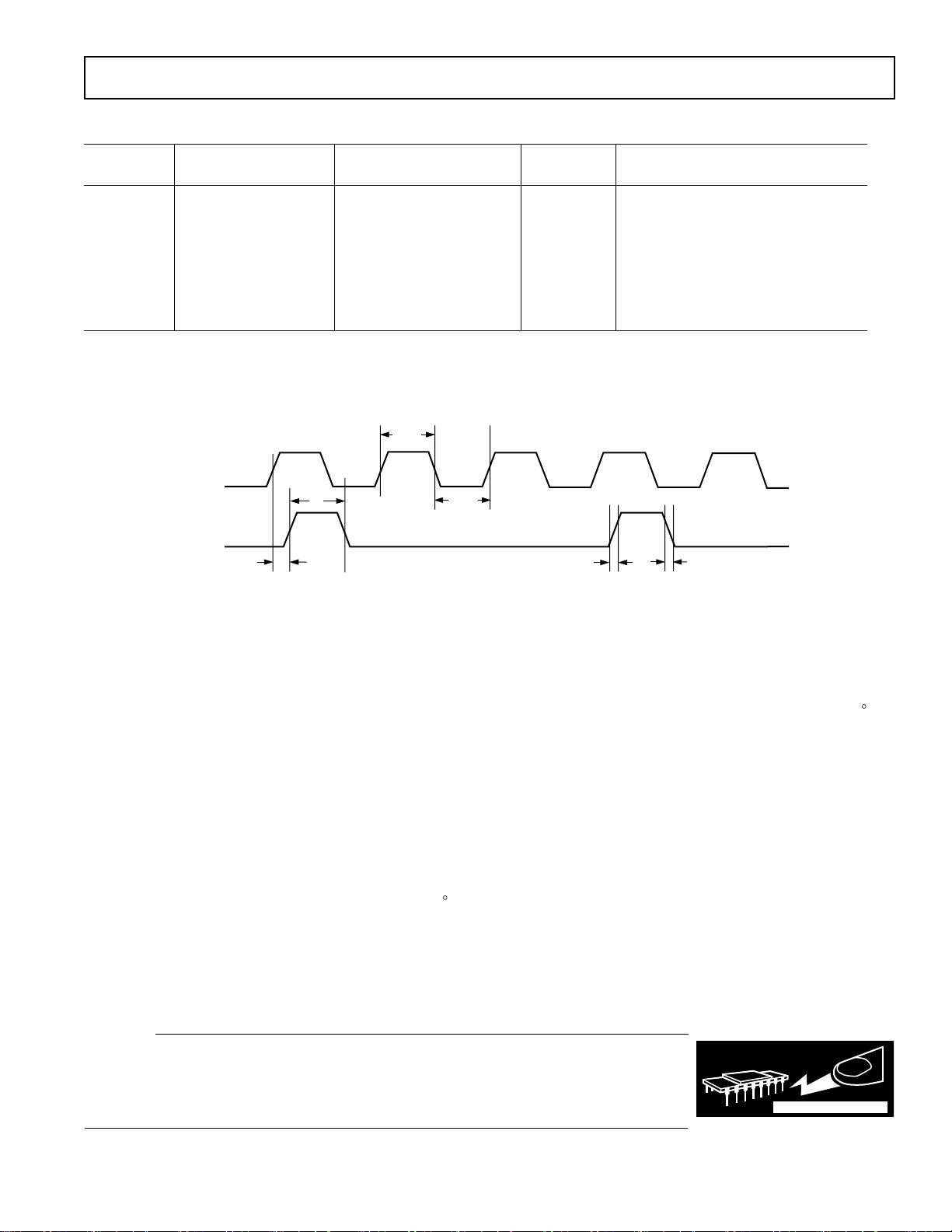
f
CLKIN
32 32 kHz min Clock Frequency
1 1 MHz max
t
HIGH
:t
LOW
40:60 40:60 min Clock Mark/Space Ratio
60:40 60:40 max
t
1
50 35 ns typ CLKIN Edge to FOUT Edge Delay
t
2
2.3 1.8 ns typ FOUT Rise Time
t
3
1.6 1.4 ns typ FOUT Fall Time
t
4
t
HIGH
± 20
t
HIGH
± 8
ns typ FOUT Pulsewidth
NOTES
1
Guaranteed by design and characterization, not production tested.
2
All input signals are specified with tr = tf = 5 ns (10% to 90% of VDD) and timed from a voltage level of (V
IL
+ V
IH
)/2.
3
See Figure 1.
Specifications subject to change without notice.
t
3
t
2
t
1
t
4
t
HIGH
t
LOW
CLKIN
FOUT
Figure 1. Timing Diagram
TIMING CHARACTERISTICS
1, 2, 3
ABSOLUTE MAXIMUM RATINGS*
(T
A
= 25°C unless otherwise noted)
VDD to GND . . . . . . . . . . . . . . . . . . . . . . . . . –0.3 V to +7 V
Analog Input Voltage to GND . . . . . . . . –0.3 V to V
DD
+ 0.3 V
Reference Input Voltage to GND . . . . . –0.3 V to V
DD
+ 0.3 V
Logic Input Voltage to GND . . . . . . . . –0.3 V to VDD + 0.3 V
FOUT Voltage to GND . . . . . . . . . . . –0.3 V to VDD + 0.3 V
Operating Temperature Range
Commercial (K Version) . . . . . . . . . . . . . . . . 0°C to +85°C
Automotive (Y Version) . . . . . . . . . . . . . . –40°C to +105°C
Storage Temperature Range . . . . . . . . . . . . –65°C to +150°C
Junction Temperature (T
J
Max) . . . . . . . . . . . . . . . . . . 150°C
SOT-23 Package
Power Dissipation . . . . . . . . . . . . . . . . . . (T
J
Max – T
A
)/θ
JA
θ
JA
Thermal Impedance . . . . . . . . . . . . . . . . . . . . . 240°C/W
Lead Temperature (10 secs) . . . . . . . . . . . . . . . . . . 300°C
Reflow Soldering
Peak Temperature . . . . . . . . . . . . . . . . . . . . 220 + 5/0°C
Time at Peak Temperature . . . . . . . . . . . . 10 sec to 40 sec
MSOP Package
Power Dissipation . . . . . . . . . . . . . . . . . (T
J
Max – T
A
)/θ
JA
θ
JA
Thermal Impedance . . . . . . . . . . . . . . . . . . . . . 206°C/W
θ
JC
Thermal Impedance . . . . . . . . . . . . . . . . . . . . . . 44°C/W
Lead Temperature (10 secs) . . . . . . . . . . . . . . . . . . . 300°C
Reflow Soldering
Peak Temperature . . . . . . . . . . . . . . . . . . . . . . 220 +5/0°C
Time at Peak Temperature . . . . . . . . . . . . . 10 sec to 40 sec
*Stresses above those listed under Absolute Maximum Ratings may cause perma-
nent damage to the device. This is a stress rating only; functional operation of the
device at these or any other conditions above those listed in the operational
sections of this specification is not implied. Exposure to absolute maximum rating
conditions for extended periods may affect device reliability.
CAUTION
ESD (electrostatic discharge) sensitive device. Electrostatic charges as high as 4000 V readily
accumulate on the human body and test equipment and can discharge without detection. Although
the AD7740 features proprietary ESD protection circuitry, permanent damage may occur on
devices subjected to high-energy electrostatic discharges. Therefore, proper ESD precautions are
recommended to avoid performance degradation or loss of functionality.
WARNING!
ESD SENSITIVE DEVICE
(VDD = 3.0 V ~ 3.6 V, 4.75 V ~ 5.25 V, GND = 0 V, REFIN = 2.5 V)
极限在 T
MIN
、T
MAX
限制在 T
MIN
、T
MAX
VDD = 3.0 V ~ 3.6 V VDD = 4.75 V至5.25 V
赫兹的最小值 时钟频率
MHz马克斯
时钟标记/空间比率
ns typ 点击边缘到FOUT边缘延迟
ns typ 四、上升时间
ns typ 四、下降时间
ns typ 输出信号脉冲宽度
由设计和特性保证,而不是生产测试。
所有输入信号都指定为tr = tf = 5 ns (VDD的10%至90%),并从 (V
IL
+V
IH
电压电平计时。
参见图1。
规格如有更改,恕不另行通知。
图1所示。时间图
时间特征
绝对最大评级*
(T
A
= 25°C(除非另有说明)
VDD,接地 . . . . . . . . . . . . . . . . . . . . . . . . . -0.3V至+ 7v
模拟输入电压到地. . . . . . . .-0.3V至 V
DD
+ 0.3V基准输入电压至GND . .
. . .-0.3 V到 V
DD
+ 0.3 V逻辑输入电压到GND . . . . . . . .-0.3 V转VDD +
0.3 V FOUT转地电压. . . . . . . . . . .-0.3 V至VDD + 0.3 V工作温度范围
商用(K版). . . . . . . . . . . . . . . .0°C + 85°C汽车(Y版本 ) . . . . . . . . . . . . . .
-40℃~ +105℃
储存温度范围. . . . . . . . . . . . -65℃~ +150℃
结温(T
J
Max ) . . . . . . . . . . . . . . . . . .150°C SOT-23封装功耗. . . . . . . . . . .
. . . . . . . (T
J
Max - T
A
)/θ
JA
JA热阻抗 . . . . . . . . . . . . . . . . . . . . .240°c / w
导致温度(10秒 ) . . . . . . . . . . . . . . . . . .300°C
再流焊
峰值温度 . . . . . . . . . . . . . . . . . . . .
峰值温度时间. . . . . . . . . . . .10秒到40秒
MSOP包
功耗 . . . . . . . . . . . . . . . . .
JA热阻抗 . . . . . . . . . . . . . . . . . . . . .206°c / w
JC热阻抗 . . . . . . . . . . . . . . . . . . . . . .44°c / w
导致温度(10秒 ) . . . . . . . . . . . . . . . . . . .300°C回流焊峰值温度. . . . . .
. . . . . . . . . . . . . . . .220 +5/0°C峰值温度时间. . . . . . . . . . . . .10秒到4
0秒
*高于绝对最大额定值的应力可能会对设备造成永久性损坏。这只是一个压力等级;不暗
示设备在这些或上述本说明书操作部分所列的任何其他条件下的功能操作。长时间暴
露在绝对最大额定值条件下可能会影响设备的可靠性。
ESD(静电放电)敏感器件。高达4000v的静电电荷很容易在人体和测试设备上积累,并且可以在不被检测到
的情况下放电。虽然AD7740具有专有的ESD保护电路,但高能静电放电可能会对器件造成永久性损坏。因
此,建议采取适当的防静电措施,避免设备性能下降或功能丧失。
静电敏感器件
剩余11页未读,继续阅读

沐风听雨_A
- 粉丝: 878
- 资源: 195
 我的内容管理
展开
我的内容管理
展开


最新资源
- 最优条件下三次B样条小波边缘检测算子研究
- 深入解析:wav文件格式结构
- JIRA系统配置指南:代理与SSL设置
- 入门必备:电阻电容识别全解析
- U盘制作启动盘:详细教程解决无光驱装系统难题
- Eclipse快捷键大全:提升开发效率的必备秘籍
- C++ Primer Plus中文版:深入学习C++编程必备
- Eclipse常用快捷键汇总与操作指南
- JavaScript作用域解析与面向对象基础
- 软通动力Java笔试题解析
- 自定义标签配置与使用指南
- Android Intent深度解析:组件通信与广播机制
- 增强MyEclipse代码提示功能设置教程
- x86下VMware环境中Openwrt编译与LuCI集成指南
- S3C2440A嵌入式终端电源管理系统设计探讨
- Intel DTCP-IP技术在数字家庭中的内容保护
资源上传下载、课程学习等过程中有任何疑问或建议,欢迎提出宝贵意见哦~我们会及时处理!
点击此处反馈


