74HC08芯片:高速CMOS四输入与门详细资料
需积分: 25 131 浏览量
更新于2024-09-11
收藏 129KB PDF 举报
"74HC08芯片英文资料"
74HC08是一款四输入与门集成电路,由先进的硅栅极CMOS(互补金属氧化物半导体)技术制造,它结合了高速性能,类似于低功耗的LS-TTL(低功耗肖特基晶体管逻辑)门电路。这款芯片设计有缓冲输出,确保高噪声免疫力,能够驱动多达10个LS-TTL负载。
74HC08的主要特点包括:
1. 典型传播延迟:7ns(tPHL,高电平到低电平的延迟时间)和12ns(tPLH,低电平到高电平的延迟时间),这表明该芯片具有较快的逻辑响应速度。
2. 高扇出能力:能驱动10个LS-TTL负载,意味着其输出端口可以为多个其他电路提供信号,而不会显著降低信号质量。
3. 静态功耗:在室温下,最大静态功耗仅为2mA,这使得74HC08适合于低功耗应用。
4. 低输入电流:每个输入端的最大电流为1mA,降低了电路的总功率消耗。
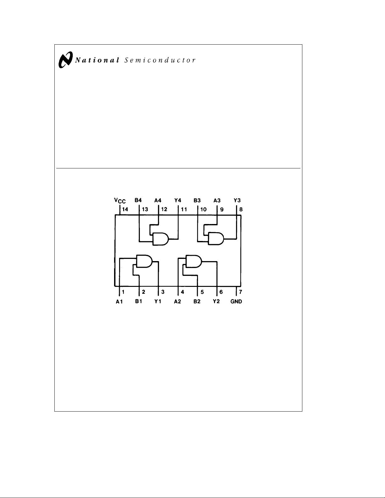
连接图显示了双列直插式封装的引脚布局,这对于实际电路板上的焊接和布局至关重要。每个与门都有两个输入端和一个输出端,这些引脚的位置在连接图中详细标出。
74HC08与标准的54LS/74LS逻辑家族在功能上和引脚排列上是兼容的,这意味着74HC08可以直接替代这些老款的逻辑门,而不需更改电路设计。所有输入端都内置了二极管钳位到VCC(电源电压)和GND(接地),以保护电路免受静电放电造成的损坏。
绝对最大额定值是设备可以承受而不造成永久性损害的极限条件,例如电源电压、输入电压、工作温度等。如果需要军用或航空航天级别的设备,应联系国家半导体销售部门进行咨询。
74HC08是一个高性能、低功耗的CMOS与门芯片,适用于需要高速逻辑操作且对功耗敏感的应用场景。其优秀的噪声免疫能力和广泛的兼容性使其成为电子设计中的常用元件。
TL/F/5297
MM54HC08/MM74HC08 Quad 2-Input AND Gate
January 1988
MM54HC08/MM74HC08
Quad 2-Input AND Gate
General Description
These AND gates utilize advanced silicon-gate CMOS tech-
nology to achieve operating speeds similar to LS-TTL gates
with the low power consumption of standard CMOS inte-
grated circuits. The HC08 has buffered outputs, providing
high noise immunity and the ability to drive 10 LS-TTL loads.
The 54HC/74HC logic family is functionally as well as pin-
out compatible with the standard 54LS/74LS logic family.
All inputs are protected from damage due to static dis-
charge by internal diode clamps to V
CC
and ground.
Features
Y
Typical propagation delay: 7 ns (t
PHL
), 12 ns (t
PLH
)
Y
Fanout of 10 LS-TTL loads
Y
Quiescent power consumption: 2 mA maximum at room
temperature
Y
Low input current: 1 mA maximum
Connection Diagram
Dual-In-Line Package
TL/F/5297–1
Top View
Order Number MM54HC08 or MM74HC08
C
1995 National Semiconductor Corporation RRD-B30M105/Printed in U. S. A.
下载后可阅读完整内容,剩余3页未读,立即下载
278 浏览量
1742 浏览量
点击了解资源详情
115 浏览量
128 浏览量
278 浏览量
370 浏览量
2021-05-12 上传

小清新Susie童鞋
- 粉丝: 0
- 资源: 1
 我的内容管理
展开
我的内容管理
展开


