1322 JOURNAL OF LIGHTWAVE TECHNOLOGY, VOL. 34, NO. 4, FEBRUARY 15, 2016
Compact Grating Coupler for 700-nm
Silicon Nitride Strip Waveguides
Xiangjie Zhao, Danping Li, Cheng Zeng, Ge Gao, Zengzhi Huang, Qinzhong Huang,
Yi Wang, Member, IEEE, Member, OSA, and Jinsong Xia, Member, IEEE, Member, OSA
Abstract—700-nm-thick silicon nitride-on-insulator (SNOI) is
widely used for nonlinear applications due to its broadband nearly
zeroflattened dispersion. Inthis paper, wepresenta grating coupler
for the TE mode of strip waveguides on 700-nm-thick SNOI. Fo-
cusing grating structure and inverse taper are combined to reduce
the footprint to 70.2 μm ×19.7 μm. The peak coupling efficiency
is −3.7 dB and the 1-dB bandwidth is 54 nm. The fabrication pro-
cess is CMOS-compatible with only one additional etching step
required.
Index Terms—Integrated optics, optical fiber couplers, silicon
nitride.
I. INTRODUCTION
I
N the era of information booming, photonic integrated cir-
cuits (PICs) find numerous applications from on-chip in-
terconnects to optical telecommunication. Silicon-on- insulator
(SOI) is the most widely used platform for realizing compact
PICs, thanks to its strong light confinement and CMOS com-
patibility [1], [2]. Silicon nitride-on-insulator (SNOI) platform
has also attracted attention recently for its better tolerance to
phase error, lower two-photon absorption loss, and better ther-
mal stability compared to Si [3]. Techniques such as apodizing
[4], blazing [5], focusing [6] and bottom mirror [7], have been
applied on SOI platform to develop efficient and compact grat-
ing couplers. There are also some grating couplers designed
for waveguides on SNOI platform [3], [8]–[10]. However, those
grating couplers are all designed on 400 nm or thinner silicon
nitride film on Silicon dioxide. Applications utilizing nonlin-
ear effect such as cascade four wave mixing, second harmonic
generation, self-phase modulation and cross-phase modulation
need at least700-nm-thick silicon nitride to introduce broadband
nearly-zero flattened dispersion [11]–[14]. Grating coupler for
700-nm-thick SNOI is necessary and has not been presented yet.
Manuscript received August 21, 2015; revised November 9, 2015; accepted
December 15, 2015. Date of publication December 16, 2015; date of current
version February 10, 2016. This work is supported in part by the Major State
Basic Research Development Program of China under Grants 2013CB632104
and 2013CB933303, the National Natural Science Foundation of China under
Grants 61335002 and 61177049, the National High Technology Research and
Development Program of China under Grant 2015AA016904, and the Program
for New Century Excellent Talents in Ministry of Education of China under
Grant NCET-12-0218. Xiangjie Zhao and Danping Li contributed equally to
this work.
The authors are with the Wuhan National Laboratory for Optoelectronics,
School of Optical and Electronic Information, Huazhong University of Sci-
ence and Technology, Wuhan 430074, China (e-mail: fhqtmso91@163.com;
danpinglioe@gmail.com; zengchengwuli@gmail.com; gaoge1991@gmail.
com; huangzengzhi@hust.edu.cn; huangqz@mail.hust.edu.cn; ywangwnlo@
mail.hust.edu.cn; jsxia@hust.edu.cn).
Color versions of one or more of the figures in this paper are available online
at http://ieeexplore.ieee.org.
Digital Object Identifier 10.1109/JLT.2015.2510025
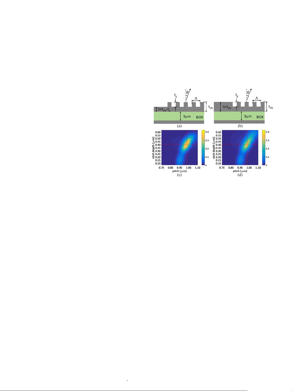
Fig. 1. Two-dimension grating coupler of (a) Geometry A with t = t
SN
− t
g
and (b) Geometry B with t = t
SN
; Contour map of to-fiber coupling effi-
ciency for various grating pitches versus etching depths for (c) Geometry A and
(d) Geometry B at 1550 nm. The red dash lines cross at the point of maximum
to-fiber coupling efficiency.
Unlike edge coupling where polished facets are required, ver-
tical grating couplers enable wafer-level testing of PICs, which
is essential for large-scale device parameter testing and high
volume manufacturing.
The main obstacle of realizing grating coupler on a thicker
slab is the excitation of higher Bloch mode in the waveguide
grating region, which severely deteriorates the coupling effi-
ciency [15]. On micrometer SOI, higher mode excitation can
be mitigated by implementing an inverse taper in front of the
grating lines [16], [17]. However, those inverse tapers have a
typical length of several hundreds of micrometers which is too
large for chip scale integration.
In this paper, we design and experimentally demonstrate, to
our knowledge, the first compact focusing grating coupler for
transverse-electric (TE) polarization on 700-nm-thick SNOI.
Through the combination of focusing grating curves and inverse
taper, the grating coupler has a footprint of 70.2 μm × 19.7 μm
and achieves coupling efficiency of −3.7 dB at C band while the
reported coupling efficiency at C band for 400-nm-thick SNOI
is −4.2 dB [9].
II. D
ESIGN
Unlike the grating on 400-nm-thick SNOI, which only has
a single (vertical) Bloch mode, the grating coupling region on
700-nm-thick SNOI supports a second order Bloch mode. The
coupling angle θ of the grating coupler, which is shown in Fig. 1
0733-8724 © 2015 IEEE. Personal use is permitted, but republication/redistribution requires IEEE permission.
See http://www.ieee.org/publications
standards/publications/rights/index.html for more information.


