30 M. Said et al. / Microprocessors and Microsystems 43 (2016) 26–46
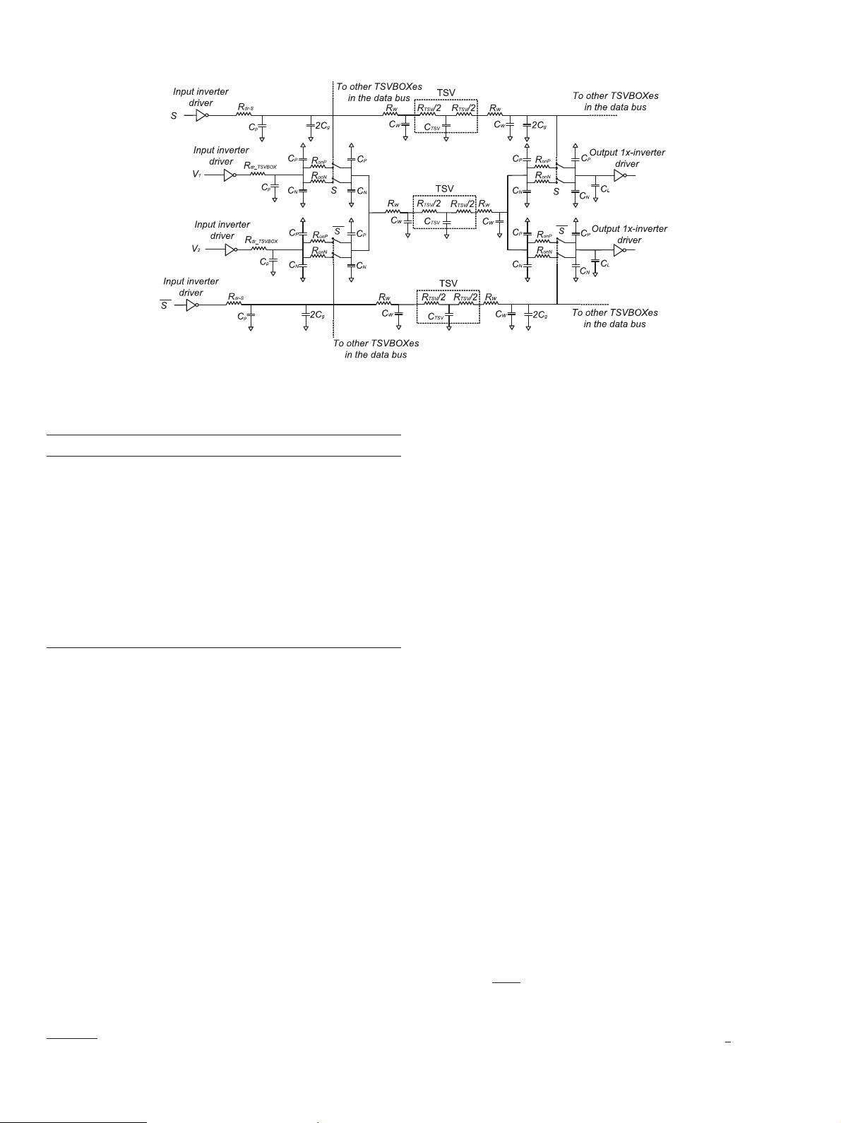
Fig. 7. TSVBOX-based 3D NoC 3D signal path.
Table 2
Transistor and other miscellaneous parasitics for 65 nm.
Transistor parasitic Unit 65 nm
C
gP
fF 0 .0689
C
gN
fF 0 .0689
C
sbP
fF 0 .0832
C
sbN
fF 0 .0819
C
dbP
fF 0 .0832
C
dbN
fF 0 .0819
R
onP
k
44 .462
R
onN
k
21 .077
C
W
fF 25
R
W
k
0 .04132
| V
thP
| V 0 .39
V
thN
V 0 .4
V
DD
V 1
C
L
fF 1 .3
C
p
fF 1 .5
It also covers the global wiring parasitics which are used for IPs
and multicore 3D-ICs
3
and the input and the output capacitances
of 1x-inverter driver shown in Fig. 4 a. Table 2 shows all the values
used in this study [23,24]
3
, noting that the length of the wires is
assumed to be 200 μm which is similar to that in [17] .
For the TSV technology, the experiments run once for
C
TSV
= 15 fF and another for C
TSV
= 500 fF to cover the whole range
of TSV capacitances and technologies, while the maximum value
for R
TSV
= 1 is selected for all cases [17] .
5.2. Transmission gate transistors
According to Uyemura [25] , transmission gate transistors are
usually selected to have minimum size. Also, as stated in [25] ,
there is no need to decrease R
onP
, hence W
P
= L
P
and K
N
= K
P
= 1 (the
sizes of NMOS and PMOS transistors, respectively) are our design
choices for the transmission gate transistors.
5.3. Threshold voltage selection for the drivers
There are two input thresholds: V
inL −max
and V
inH−min
. V
inL −max
is the maximum low input voltage required to switch PMOS ON
and NMOS OFF at the same time. Therefore if V
in
≤ V
inL −max
, NMOS
3
http://www.itrs.net/reports.html .
will be OFF and PMOS will be ON . The other threshold voltage is
V
inH−min
, which is the minimum high input voltage required to
switch NMOS ON and PMOS OFF at the same time, therefore if V
in
≥ V
inH−min
, NMOS will be ON and PMOS will be OFF . Depending on
the previous definitions, the thresholds can be selected as follows
V
inL −max
= V
thN
, V
inH−min
= V
DD
− | V
thP
| (3)
6. Timing requirements’ analysis
In this section all timing analysis related to TSVBOX-based 3D
NoC is discussed. Timing requirements’ analysis include 3D path
delays, how to choose the selection signal period T
S
, and the rela-
tion between S and the main clock signal.
6.1. 3D signal path Elmore-delay model
The 3D signal path delay for data and S signals in conventional
and TSVBOX-based 3D NoCs can be approximated using first order
Elmore-delay model [23] . The delay for data signals is the time re-
quired for the 3D data signal to reach V
inH−min
= V
DD
−| V
thP
|. The 3D
data signals passing through the conventional or the TSVBOX 3D
paths are to be destined to a 1x-inverter driver load, as shown in
Figs. 6 and 7 , respectively. For S signal, the delay is the time re-
quired for S to reach max( V
thN
, | V
thP
|), because S is destined to the
transmission gate transistors ( PMOS or NMOS ). Hence the voltage
required for S signal to switch either NMOS or PMOS ON is V
thN
or
| V
thP
|, respectively. The maximum of these two voltages is selected
to meet both conditions.
According to Section 5 , the wiring and TSV resistances are in or-
der of ohms, therefore their contribution to the total delay is neg-
ligible. Thus these resistances will be ignored to simplify the delay
analysis in this paper.
6.1.1. Conventional 3D NoC 3D signal delay
Referring to Fig. 6 , the conventional 3D NoC 3D signal path de-
lay ( T
d−Con v
) can be approximated using Elmore-delay as follows:
T
d−Con v
= ln
V
DD
| V
thP
|
·
(
R
dr−Con v
· (C
p
+ 2 C
W
+ C
T SV
+ C
L
)
)
(4)
6.1.2. TSVBOX-based 3D NoC 3D signal delay
The TSVBOX has two different paths according to the values
of the S signal. Fig. 8 shows the situation when S = 1 ( S = 0) that


