英飞凌TLF4277EL低 dropout线性稳压器中文规格手册
需积分: 0 169 浏览量
更新于2024-06-23
收藏 1.37MB PDF 举报
TLF4277EL是一款由英飞凌(INFINEON)公司生产的低降压线性电压调节器,专为汽车应用设计。该芯片具有集成电流监控功能,提供了全面的性能参数和保护特性,旨在确保系统的稳定性和可靠性。
**1. 产品概述**
TLF4277EL的核心是其低阻抗线性稳压器,它能够将输入电压稳定转换为可调的输出电压,适用于对电源电压需求敏感的应用。其设计目标是提供高效能、低噪声和小型化的解决方案。
**2. 块级结构与配置**
- **3.1. Pin Assignment**:芯片的引脚分配清晰明确,包括电源输入、接地、输出以及控制和监测信号,方便用户根据需要连接和配置电路。
- **3.2. Pin Definitions and Functions**:每个引脚的功能被详细定义,如电源输入的Vin、输出的Vout、以及监控和控制信号如EN、LDO_MODE等。
**3. 性能特性**
- **4.1. Absolute Maximum Ratings**:提供了芯片在极限工作条件下的电气和机械参数,如最高输入电压、最大输出电流和温度限制等。
- **4.2. Functional Range**:描述了正常运行时的性能范围,包括电压调节精度、负载调整率等关键指标。
- **4.3. Thermal Resistance**:阐述了芯片的热阻,这对于评估其在不同环境下的散热性能至关重要。
**4. 电压调节器功能**
- **5.1. Description Voltage Regulator**:详述了电压调节器的工作原理和操作方法,包括输入电压的适应范围和输出电压的可调范围。
- **5.2. Electrical Characteristics Voltage Regulator**:列出电压调节器的关键电气特性,如最大输出电流、输出电压调整范围和噪声水平等。
- **5.3. Application Information**:针对设置可变输出电压提供了实用的指导和建议,帮助用户优化电路设计。
**5. 电流消耗与保护**
- **6.1. Electrical Characteristics Current Consumption**:给出了电流消耗的详细数据,包括静态和动态电流,这对于电源管理至关重要。
- **6.2. Typical Performance Graphs Current Consumption**:展示典型性能曲线,展示电流随负载变化的情况,帮助用户理解实际应用中的功耗情况。
**6. 监控与保护功能**
- **7.1. Current and Protection Monitors**:介绍内置的线性电流监控器、可调输出电流限制、过电压检测以及热关断检测功能,这些功能用于保护电路免受过载和过热的影响。
- **7.2. Electrical Characteristics of Monitoring Functions**:列出了这些保护功能的响应时间和阈值设定,以便用户根据需要进行调整。
TLF4277EL是一款针对汽车电子应用的高效率、集成度高的线性电压调节器,具有优良的电流控制能力和保护特性,为系统设计者提供了灵活且可靠的电源解决方案。在使用时,需注意芯片的极限工作条件、性能特性和保护功能的正确配置,以确保设备的稳定运行。
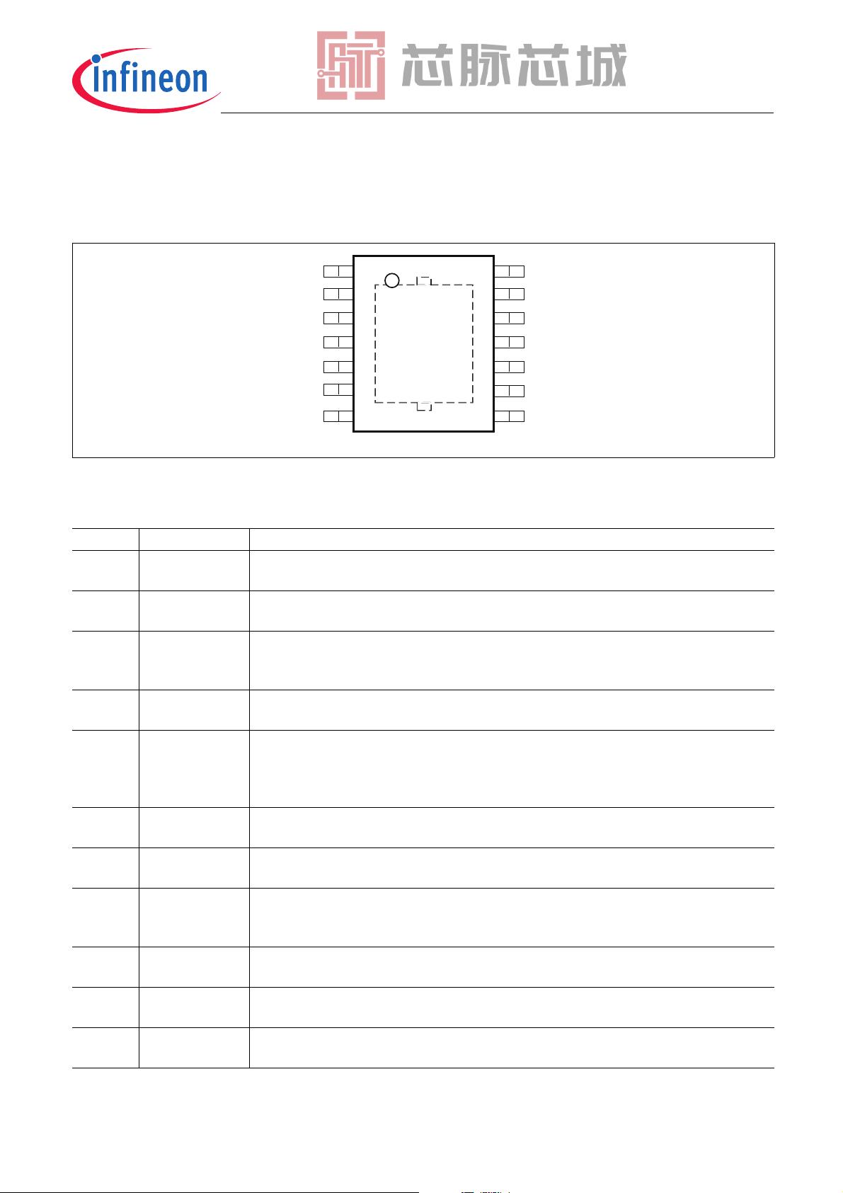
TLF4277
Pin Configuration
Data Sheet 5 Rev. 1.02, 2011-07-05
3 Pin Configuration
3.1 Pin Assignment
Figure 2 Pin Configuration (top view)
3.2 Pin Definitions and Functions
Pin Symbol Function
1CS2 Current Sense In 2
current monitor and power stage input
3CS1 Current Sense In 1
current monitor input
5I IC Supply
Place a capacitor from I (Pin 5) to GND close to the IC for compensating line
influences.
7CSO Current Sense Out
current monitor and status output
8EN Enable
high signal enables the regulator;
low signal disables the regulator;
connect to I, if the Enable function is not needed
10 GND Ground
connect pin to PCB and heat sink area
12 ADJ Voltage Adjust
connect an external voltage divider to configure the output voltage
14 Q Regulator Output
connect a capacitor between Q (Pin 8) and GND close to the IC pins, respecting the
values given for its capacitance C
Q
and ESR in the table Chapter 4.2
PAD
Heat sink
connect to PCB heat sink area and GND
2,4,6 NC Not Connected
Internally not connected; Connect to PCB GND
9,11,13 NC Not Connected
Internally not connected; Connect to PCB GND
Q
EN
NC
GND
NC
ADJ
NC
CS2
CSO
NC
I
NC
CS1
NC
1
2
3
4
5
6
7
14
9
10
11
12
13
8
TLF4277_PINCONFIG_SSOP-14.SVG
剩余21页未读,继续阅读
2023-07-07 上传
2023-07-06 上传
2023-07-07 上传
2023-07-07 上传
2023-07-10 上传
2023-07-10 上传

芯脉芯城
- 粉丝: 4
- 资源: 4030
 我的内容管理
展开
我的内容管理
展开


最新资源
- Java集合ArrayList实现字符串管理及效果展示
- 实现2D3D相机拾取射线的关键技术
- LiveLy-公寓管理门户:创新体验与技术实现
- 易语言打造的快捷禁止程序运行小工具
- Microgateway核心:实现配置和插件的主端口转发
- 掌握Java基本操作:增删查改入门代码详解
- Apache Tomcat 7.0.109 Windows版下载指南
- Qt实现文件系统浏览器界面设计与功能开发
- ReactJS新手实验:搭建与运行教程
- 探索生成艺术:几个月创意Processing实验
- Django框架下Cisco IOx平台实战开发案例源码解析
- 在Linux环境下配置Java版VTK开发环境
- 29街网上城市公司网站系统v1.0:企业建站全面解决方案
- WordPress CMB2插件的Suggest字段类型使用教程
- TCP协议实现的Java桌面聊天客户端应用
- ANR-WatchDog: 检测Android应用无响应并报告异常
