英飞凌芯片TLF1963TE中文规格书.pdf
需积分: 5 66 浏览量
更新于2023-11-24
收藏 1.76MB PDF 举报
TLF1963TE 英飞凌芯片 INFINEON 中文版规格书手册.pdf 是一份详细介绍 TLF1963TE 产品的规格书手册,内容包括产品概述、方框图、引脚配置、引脚分配和功能定义等。该手册于2012年11月08日发布,版本为1.0。TLF1963TE 是一款低压差线性稳压器,用于汽车电源系统。该手册为英飞凌芯片 INFINEON 公司出品,详细介绍了 TLF1963TE 的性能和技术参数,对于使用该产品的工程师和研发人员具有重要的参考价值。
TLF1963
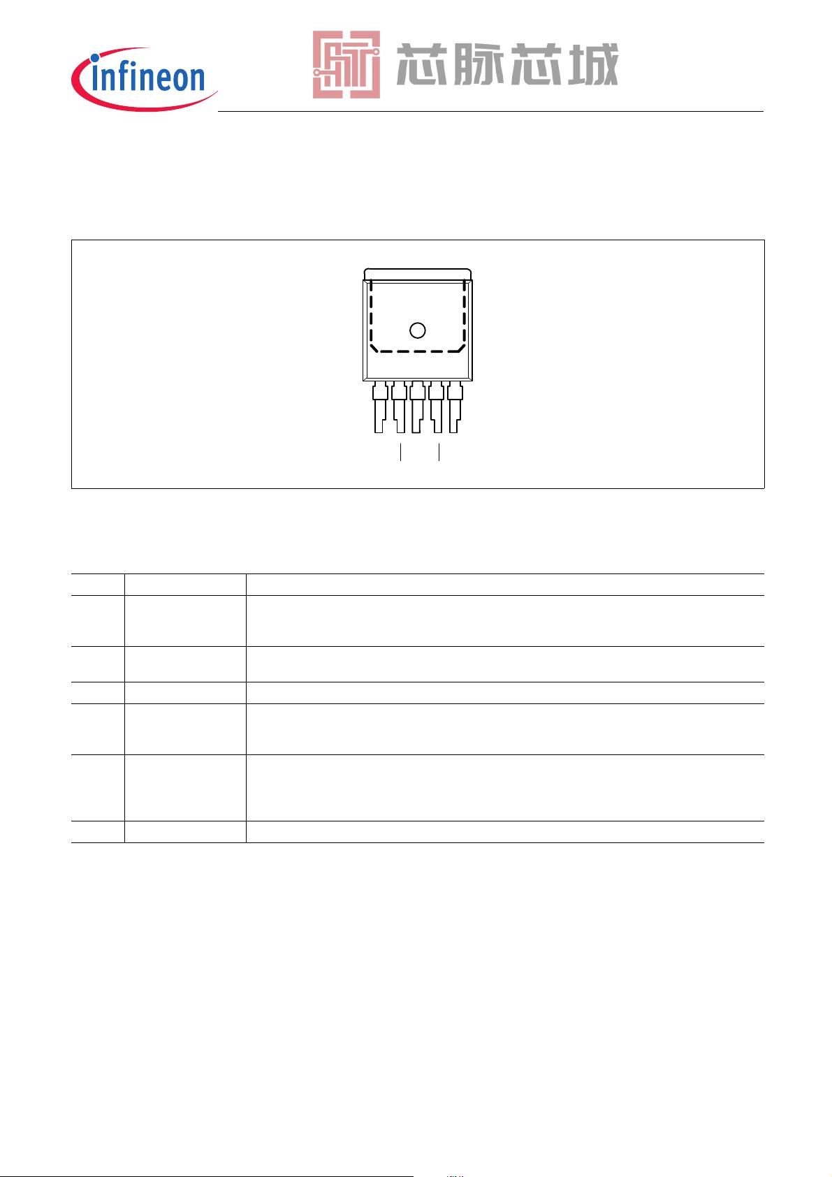
Pin Configuration
Data Sheet 5 Rev. 1.0, 2012-11-08
3 Pin Configuration
3.1 Pin Assignment TLF1963TB
Figure 2 Pin Configuration PG-TO263-5
3.2 Pin Definitions and Functions TLF1963TB
Pin Symbol Function
1EN
Enable;
A low signal disables the IC. A high signal switches it on.
Connect to the input I, if enable functionality is not required.
2I
Input voltage;
IC supply. For compensating line influences, a capacitor close to the IC pins is recommended.
3GND
Ground
4Q
Output voltage;
Connect a capacitor between Q and GND close to the IC terminals, respecting the values
given for its capacitance
C
Q
and ESR given in the table “Functional Range” on Page 8
5ADJ
Adjust Input;
Connect an external voltage divider from Q to GND to determine the output voltage.
By connecting the output pin Q directly to the adjust pin ADJ without resistors an ouput
voltage equal to the reference voltage
V
ADJ
= 1.21 V is determined.
TAB GND
Ground
51
GND
GND
EN
IQ
ADJ
剩余23页未读,继续阅读
2023-07-10 上传
2023-07-07 上传
2023-07-07 上传
2023-05-10 上传
2023-09-29 上传
2023-07-28 上传
2023-09-29 上传
2023-05-10 上传
2023-04-01 上传

芯脉芯城
- 粉丝: 4
- 资源: 4030
 我的内容管理
展开
我的内容管理
展开


最新资源
- Angular实现MarcHayek简历展示应用教程
- Crossbow Spot最新更新 - 获取Chrome扩展新闻
- 量子管道网络优化与Python实现
- Debian系统中APT缓存维护工具的使用方法与实践
- Python模块AccessControl的Windows64位安装文件介绍
- 掌握最新*** Fisher资讯,使用Google Chrome扩展
- Ember应用程序开发流程与环境配置指南
- EZPCOpenSDK_v5.1.2_build***版本更新详情
- Postcode-Finder:利用JavaScript和Google Geocode API实现
- AWS商业交易监控器:航线行为分析与营销策略制定
- AccessControl-4.0b6压缩包详细使用教程
- Python编程实践与技巧汇总
- 使用Sikuli和Python打造颜色求解器项目
- .Net基础视频教程:掌握GDI绘图技术
- 深入理解数据结构与JavaScript实践项目
- 双子座在线裁判系统:提高编程竞赛效率
