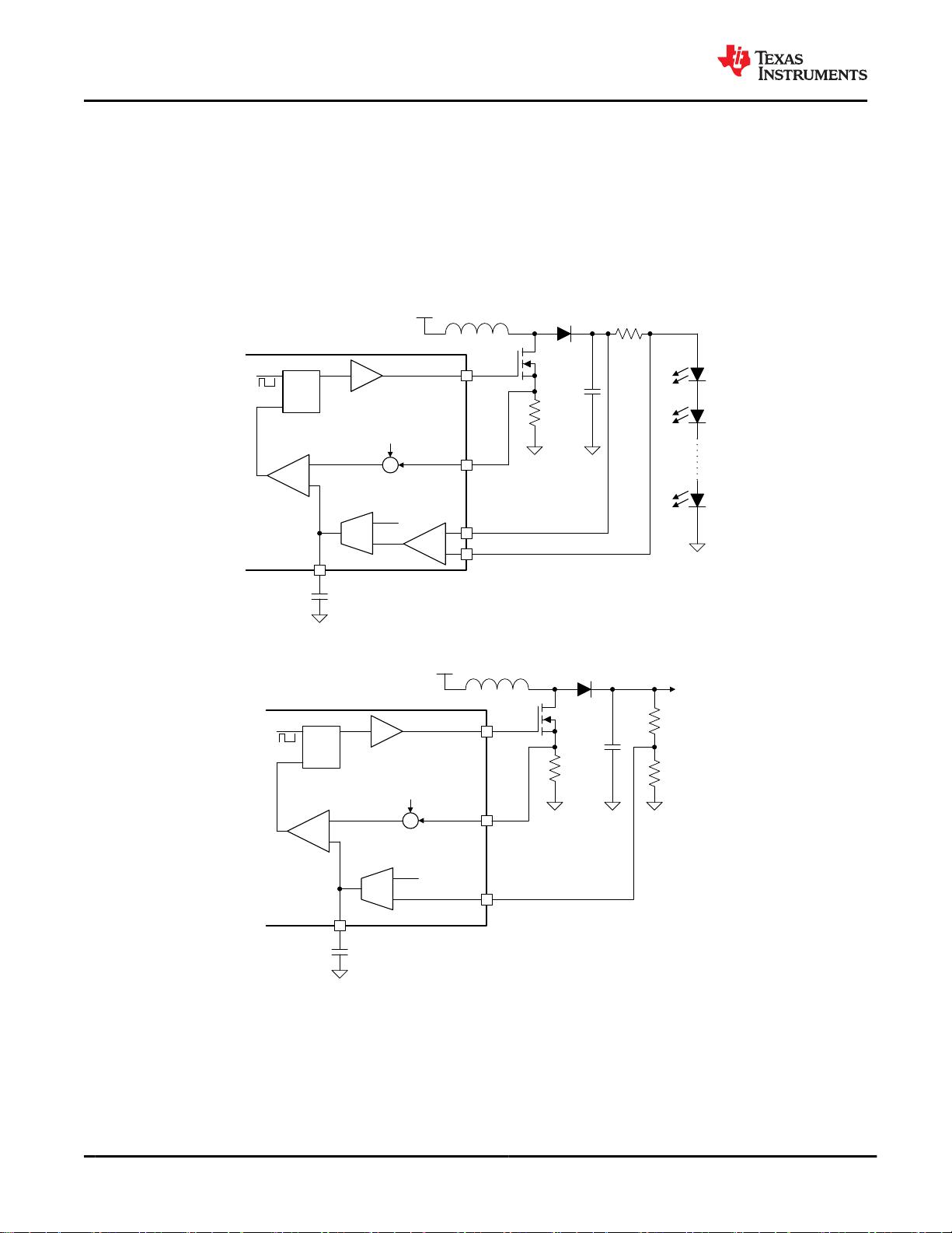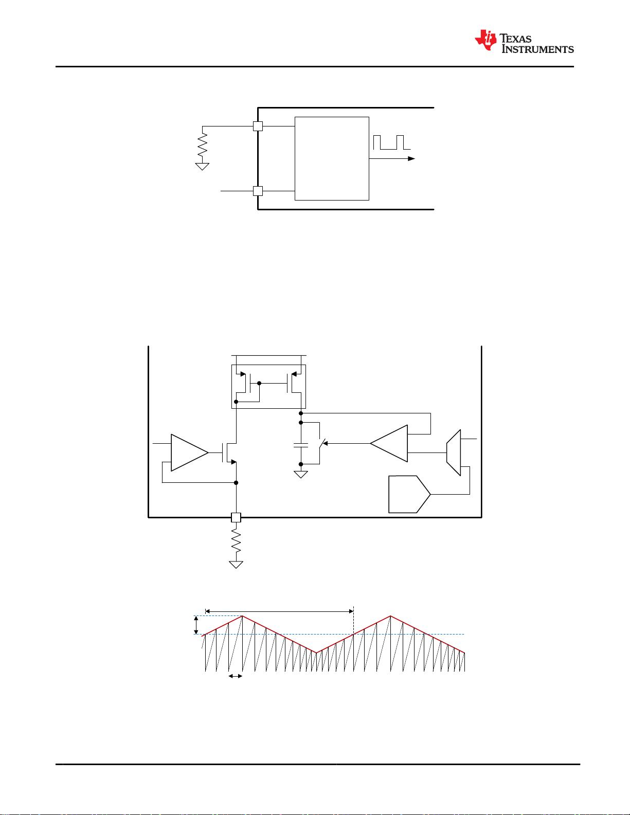
图 7-3. PCM Control and Ramp Compensation
7.3.1 Device Enable
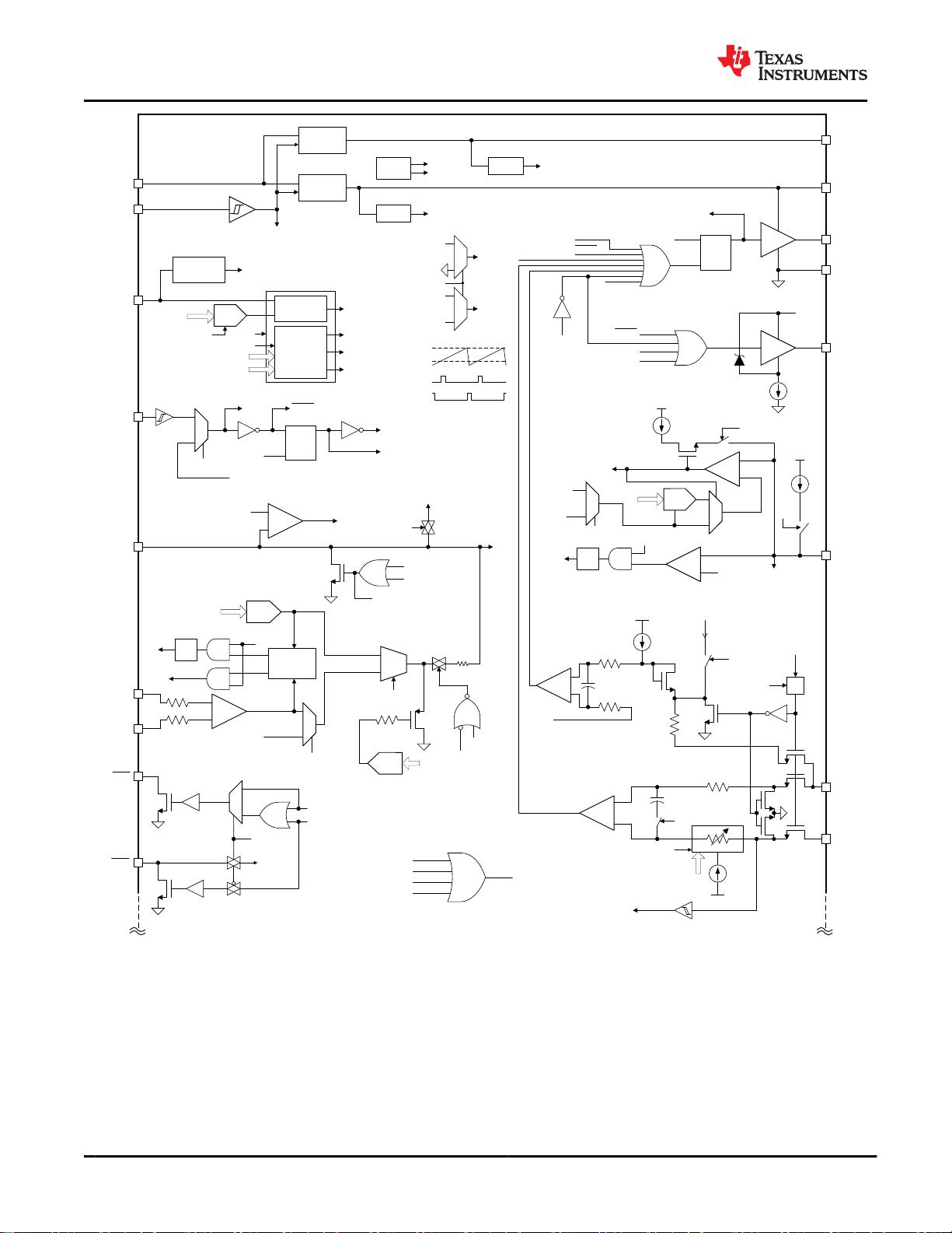
The TPS92682-Q1 can be enabled or disabled by the EN pin or the software enable bits. When EN pin is pulled
low, the device enters shutdown state, where the quiescent current of the device is decreased to I
IN-SHDN
. In
shutdown state, the internal regulators are turned off and the registers are reset. When the voltage on the enable
pin is increased above the voltage threshold of V
EN
, the two channels can be enabled. In addition to the EN pin,
there are two enable bits for the two channels of the TPS92682-Q1 as shown in
表 7-2. In order for each
channel to be turned on, the associated CHxEN bit must be set to "1" in EN Register.
In addition to the EN pin and the CHxEN bits, the PWMx signals (hardware or software) must be set high and the
associated CHxIADJ must be set to a value greater than eight (refer to the CH1IADJ Register) in order for the
associated channel to be turned on.
7.3.2 Internal Regulator and Undervoltage Lockout (UVLO)
The device incorporates 65-V input voltage rated linear regulators to generate the 7.5-V (typical) VCC bias
supply, the 5-V (typical) VDD supply, and other internal reference voltages. The device monitors the VCC output
to implement UVLO protection. Operation is enabled when VCC exceeds the 4.5-V (typ) threshold and is
disabled when VCC drops below the 4.1-V (typical) threshold. The UVLO comparator provides a hysteresis to
avoid chatter during transitions. The UVLO thresholds are internally fixed and cannot be adjusted. An internal
current limit circuit is implemented to protect the device during VCC pin short-circuit conditions. The VCC supply
powers the internal circuitry and the N-channel gate driver outputs, GATEx. Place a bypass capacitor in the
range of 2.2 μF to 4.7 μF across the VCC output and GND to ensure proper operation. The regulator operates
in dropout when input voltage VIN falls below 7.5 V. The VCC is a regulated output of the internal regulator and
is not recommended to be driven with an external power supply.
The internal VDD regulator is used to generate supply voltage for various internal analog and digital circuits. The
supply current is internally limited to protect the device from output overload and short-circuit conditions. Place a
bypass capacitor in the range of 2.2
μF to 4.7 μF across the VDD output to GND to ensure proper operation.
The POR circuit of the device is placed at the output of the VDD regulator. The POR rise and fall thresholds are
provided in the Electrical Characteristics.
7.3.3 Oscillator
The internal clock frequency of the TPS92682-Q1 device is programmable by a single external resistor,
connected between the RT pin and the GND. The relationship between the resistor R
T
and the internal main
clock (CLK
M
) frequency is shown in 方程式 1 and Channel Switching Frequency F
SW
vs R
T
Resistance.
(1)
The relationship between the channel clock, CHx
CLK
(or the channel switching frequency f
SW
), and f
CLKM
is
shown in the SWDIV Register section. TI recommends a switching frequency setting between 100 kHz to 700
kHz for best efficiency and for optimal performance over input and output voltage operating range. Operation at
higher switching frequencies requires careful selection of N-channel MOSFET characteristics as well as detailed
analysis of switching losses.
www.ti.com.cn
TPS92682-Q1
ZHCSK35C – MARCH 2019 – REVISED MARCH 2021
Copyright © 2021 Texas Instruments Incorporated
Submit Document Feedback
19
Product Folder Links: TPS92682-Q1


