VII-3
A
Monolithic
HEMT
Regulated Self-biased LNA
K.W.
Kobayashi,
R.
Esfandiari,
B.
Nelson, K. Minot,
W.
Jones,
M.
Biendenbender,
R.
Lai, K.L. Tan, and J.B. Berenz
TRW
Electronic and Technology Division
One Space Park
Redondo Beach,
CA
90278
ABSTRACT
This
work benchmarks the first demonstration of a monolithic
HEMT LNA design which incorporates active regulated self-bias. The
HEMT LNA bias current can be maintained to within
f
3%
variation
over a process threshold variation (Vgs)
of
f
0.5 Volt. The bias
circuitry regulates the bias current to within
1.5%
over a 100°C
temperature range. The amplifier has a nominal gain of 10 dB and a
noise figure of 2.5 dB over a
1-10
GHz bandwidth. Across several
wafers with a threshold voltage spread of
0.5
Volts, the active bias-
regulated LNA maintains repeatable gain and noise figure which varies
by less
than
1
dB and
0.75
dB respectively. This monolithic regulated
self-biased LNA demonstration sheds new light on the producibility
and
reliability of HEMT MMICs and their applications.
Introduction
The high performance of
HEMTs
are currently driven by
state-of-the-art MBE material growth and electron beam lithography
techniques, as well
as
an advanced gate etch process. All of these
critical techniques
are
utilized to their fullest capability to obtain the
highest fT'S
and
lowest noise figures. A major ramification
of
Ux
HEMT fabrication technology is the widely varying gate threshold
voltages. For practical applications,
HEMT
MMICs require a circuit
means for self-biasing the HEMT which is tolerant
of
the device dc
threshold voltage variations.
Resistive self-bias techniques are commonly used in
MESFET
technology and can be applied to HEMTs; however, the HEMT
implementation will
be
more bias sensitive due to the transistor's
widely varying threshold characteristics. Active HEMT current source
techniques will also be sensitive to process variations and requires
depletion mode HEMT devices. A current source topology has been
implemented in HEMTs and achieves
f
20%
bias current variation
over
a
f
0.2
Volts threshold variation
[I].
This topology operates off
a
3.3
V supply. A current mimr topology which has been
used
in a
JFET
amplifier achieves
f
25%
current variation for a
f
0.2
V
threshold range
121.
Similar performance is expected of a HEMT
current-mimr bias implementation.
94CH3351-4/94/0000-0121$01
.OO
0
1994
IEEE
In many applications, current regulation on the order off 2-
5%
is required for both depletion and enhancement mode HEMTs.
Thus
the
bias techniques described above may not
be
an adequate self-
bias solution.
In
addition, temperature compensation may
be
a key
requirement. An elegant solution would be to monolithically integrate a
HEMT
regulator.
The work presented in
this
paper describes the design and
performance of a monolithic HEMT current regulator which is
integrated with a low noise amplifier to provide bias regulation over
temperature
and
HEMT
pmss variations.
HEMT Monolithic Regulated
LNA
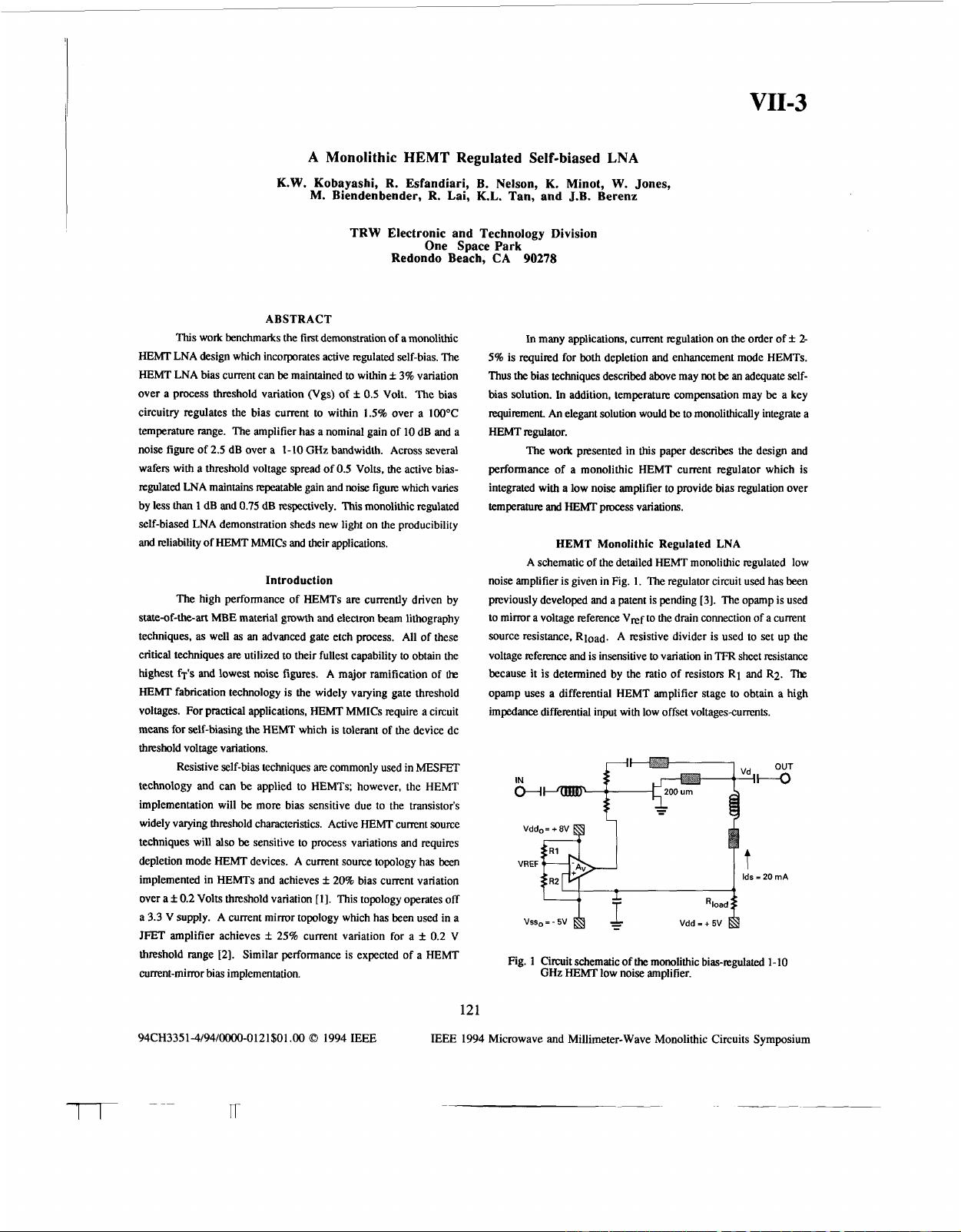
A schematic of the detailed HEMT monolithic regulated low
noise amplifier is given in Fig. 1. The regulator circuit
used
has been
previously developed and a patent is pending
[3].
The opamp is used
to mimr a voltage reference Vref to the drain connection of a current
source resistance, Rload. A resistive divider is used to set up the
voltage reference and
is
insensitive
to
variation in
TFR
sheet resistance
because it is determined by the ratio of resistors R1 and R2.
The
opamp
uses
a differential HEMT amplifier stage to obtain a high
impedance differential input with low offset voltagescurrents.
Vddo=+8V
@
I
vREFp;
vss,
-U
=
-
5v
t
Ids
=
20
mA
Vdd
=
+
5V
Fig.
1
Circuit schematic of
the
monolithic bias-regulated
1-10
GHz
HEMT
low noise amplifier.
121
IEEE
1994
Microwave and Millimeter-Wave Monolithic Circuits Symposium
n


