mA
MAX517/MAX518/MAX519
2-Wire Serial 8-Bit DACs with
Rail-to-Rail Outputs
4 _______________________________________________________________________________________
Note 1: For the MAX518 (full-scale = V
DD
) the last three codes are excluded from the TUE and DNL specifications, due to the limited
output swing when loaded with 10kΩ to GND.
Note 2: Input resistance is code dependent. The lowest input resistance occurs at code = 55 hex.
Note 3: Input capacitance is code dependent. The highest input capacitance occurs at code FF hex.
Note 4: V
REF_
= 4V
P-P
, 10kHz. Channel-to-channel isolation is measured by setting the code of one DAC to FF hex and setting the
code of all other DACs to 00 hex.
Note 5: V
REF_
= 4Vp-p, 10kHz, DAC code = 00 hex.
Note 6: Guaranteed by design.
Note 7: I
2
C compatible mode. R
PULLUP
= 1.7kΩ.
Note 8: Output settling time is measured by taking the code from 00 hex to FF hex, and from FF hex to 00 hex.
Note 9: A master device must provide a hold time of at least 300ns for the SDA signal (referred to V
IL
of the SCL signal) in order to
bridge the undefined region of SCL’s falling edge.
Note 10: Cb = total capacitance of one bus line in pF. t
R
and t
F
measured between 0.3V
DD
and 0.7V
DD
.
Note 11: Input filters on the SDA and SCL inputs suppress noise spikes less than 50ns.
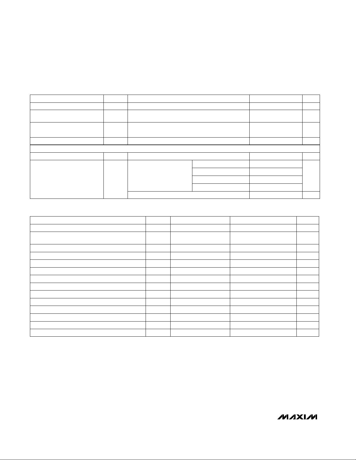
Hold Time, (Repeated) Start Condition t
HD, STA
0.6 µs
Low Period of the SCL Clock t
LOW
1.3 µs
High Period of the SCL Clock t
HIGH
0.6
PARAMETER SYMBOL MIN TYP MAX UNITS
Serial Clock Frequency f
SCL
0400kHz
Bus Free Time Between a STOP and a
START Condition
t
BUF
1.3 µs
CONDITIONS
µs
Setup Time for a Repeated START Condition t
SU, STA
0.6 µs
Data Hold Time t
HD, DAT
0 0.9 µs
Data Setup Time t
SU, DAT
100
(Note 9)
ns
Fall Time of SDA Transmitting t
F
20 + 0.1Cb 250 ns
Setup Time for STOP Condition t
SU, STO
0.6 µs
Capacitive Load for Each Bus Line Cb 400
I
SINK
≤ 6mA (Notes 7, 10)
pF
Rise Time of Both SDA and SCL Signals, Receiving t
R
20 + 0.1Cb 300 ns
Fall Time of Both SDA and SCL Signals, Receiving t
F
20 + 0.1Cb 300
(Note 10)
(Note 10) ns
Pulse Width of Spike Suppressed t
SP
050(Notes 6, 11) ns
TIMING CHARACTERISTICS
(V
DD
= 5V ±10%, T
A
= T
MIN
to T
MAX
, unless otherwise noted. Typical values are T
A
= +25°C.)
ELECTRICAL CHARACTERISTICS (continued)
(V
DD
= 5V ±10%, V
REF_
= 4V (MAX517, MAX519), R
L
= 10kΩ, C
L
= 100pF, T
A
= T
MIN
to T
MAX
, unless otherwise noted.
Typical values are T
A
= +25°C.)
PARAMETER SYMBOL MIN TYP MAX UNITSCONDITIONS
Digital-Analog Glitch Impulse 12Code 128 to 127 nV-s
Signal to Noise + Distortion
Ratio (MAX517, MAX519)
SINAD 87
V
REF_
= 4Vp-p at 1kHz, V
DD
= 5V,
Code = FF hex
dB
Multiplying Bandwidth
(MAX517, MAX519)
1 MHz
Wideband Amplifier Noise 60 µV
RMS
Supply Voltage V
DD
4.5 5.5 V
1.5 3.0
MAX517E/M
MAX517C
2.5 5
1.5 3.5
V
REF_
= 4Vp-p, 3dB bandwidth
Supply Current
Normal mode, output(s)
unloaded, all digital inputs
at 0V or V
DD
2.5 6
MAX518C, MAX519C
MAX518E/M, MAX519E/M
I
DD
Power-down mode 420µA
POWER REQUIREMENTS


