
8
TCAN330
,
TCAN332
,
TCAN334
,
TCAN337
TCAN330G
,
TCAN332G
,
TCAN334G
,
TCAN337G
SLLSEQ7E –DECEMBER 2015–REVISED DECEMBER 2019
www.ti.com
Product Folder Links: TCAN330 TCAN332 TCAN334 TCAN337 TCAN330G TCAN332G TCAN334G TCAN337G
Submit Documentation Feedback Copyright © 2015–2019, Texas Instruments Incorporated
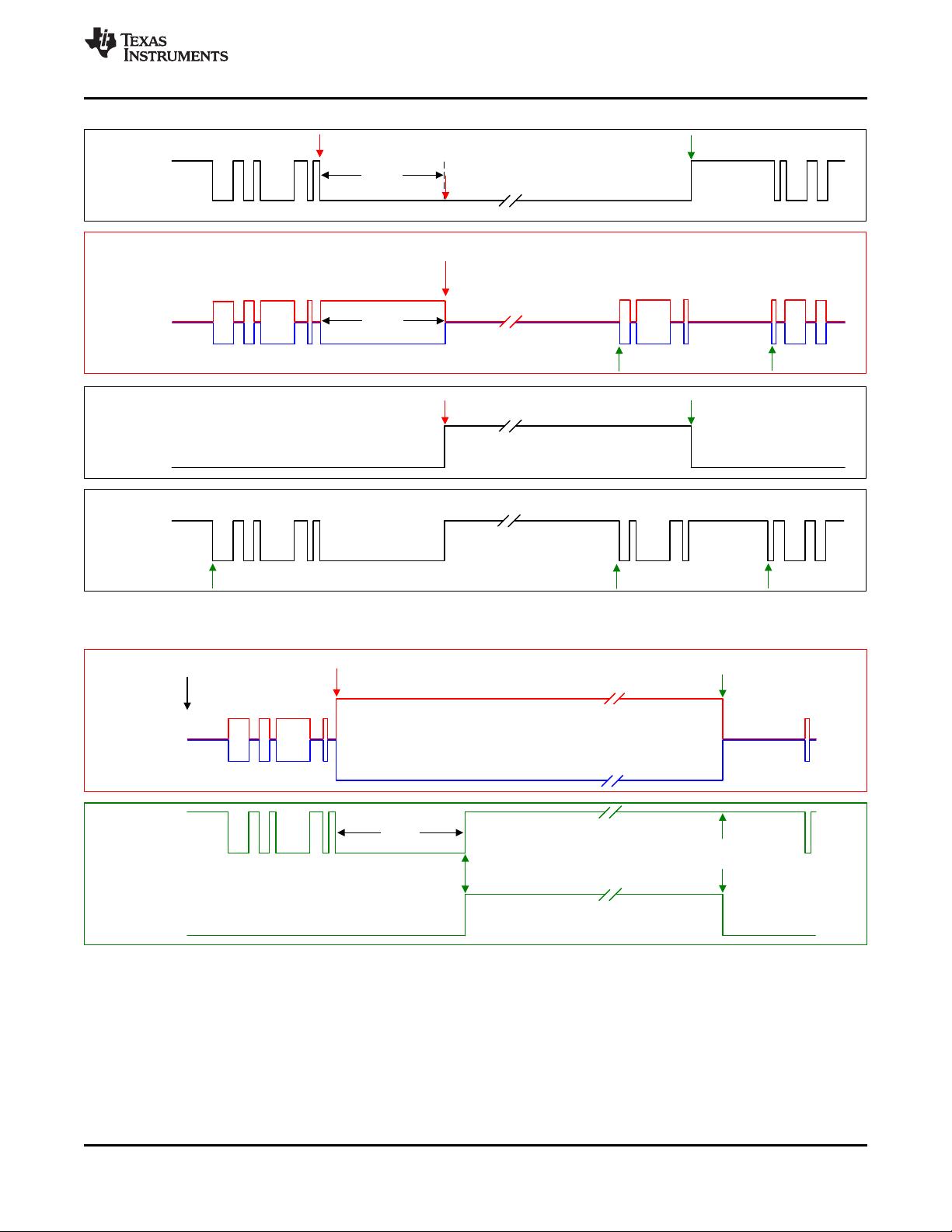
(1) The TXD dominant time out (t
TXD_DTO
) disables the driver of the transceiver once the TXD has been dominant longer than t
TXD_DT
O,
which releases the bus lines to recessive, preventing a local failure from locking the bus dominant. The driver may only transmit
dominant again after TXD has been returned HIGH (recessive). While this protects the bus from local faults, locking the bus dominant, it
limits the minimum data rate possible. The CAN protocol allows a maximum of eleven successive dominant bits (on TXD) for the worst
case, where five successive dominant bits are followed immediately by an error frame. This, along with the t
TXD_DTO
minimum, limits the
minimum bit rate. The minimum bit rate may be calculated by: Minimum Bit Rate = 11/ t
TXD_DTO
= 11 bits / 1.2 ms = 9.2 kbps.
(2) The RXD timeout (t
RXD_DTO
) disables the RXD output in the case that the bus has been dominant longer than t
RXD_DTO
, which releases
RXD pin to the recessive state (high), thus preventing a dominant bus failure from permanently keeping the RXD pin low. The RXD pin
will automatically resume normal operation once the bus has been returned to a recessive state. While this protects the protocol
controller from a permanent dominant state, it limits the minimum data rate possible. The CAN protocol allows a maximum of eleven
successive dominant bits (on RXD) for the worst case, where five successive dominant bits are followed immediately by an error frame.
This, along with the t
RXD_DTO
minimum, limits the minimum bit rate. The minimum bit rate may be calculated by: Minimum Bit Rate = 11 /
t
RXD_DTO
= 11 bits / 1.6 ms = 6.9 kbps.
8.6 Switching Characteristics
over operating free-air temperature range (unless otherwise noted)
PARAMETER TEST CONDITIONS MIN TYP MAX UNIT
Device Switching Characteristics
t
PROP(LOOP)
Total loop delay, driver input (TXD) to
receiver output (RXD), recessive to
dominant and dominant to recessive
See Figure 23, S, STB and SHDN = 0 V,
R
L
= 60 Ω, C
L
= 100 pF, C
L(RXD)
= 15 pF
100 135 ns
t
PROP(LOOP)
Total Loop delay in highly loaded
network
See Figure 23, S, STB and SHDN = 0 V,
R
L
= 120 Ω, C
L
= 200 pF,
C
L(RXD)
= 15 pF
120 180 ns
t
BUS_SYM_2
2 Mbps transmitted recessive bit width
See Figure 24, S or STB = 0 V, R
L
= 60
Ω, C
L
= 100 pF, C
L(RXD)
= 15 pF,
t
BIT
= 500 ns
TCAN330G, TCAN332G, TCAN334G
and TCAN337G only
435 530 ns
t
REC_SYM_2
2 Mbps received recessive bit width 400 550 ns
Δt
SYM_2
2 Mbps receiver timing symmetry
(t
REC_SYM_2
- t
BUS_SYM_2
)
–65 40 ns
t
BUS_SYM_5
5 Mbps transmitted recessive bit width
See Figure 24, S or STB = 0 V, R
L
= 60
Ω, C
L
= 100 pF, C
L(RXD)
= 15 pF,
t
BIT
= 200 ns
TCAN330G, TCAN332G, TCAN334G
and TCAN337G only
155 210 ns
t
REC_SYM_5
5 Mbps received recessive bit width 120 220 ns
Δt
SYM_5
5 Mbps receiver timing symmetry
(t
REC_SYM_5
- t
BUS_SYM_5
)
–45 15 ns
t
MODE
Mode change time
See Figure 21 and Figure 22.
R
L
= 60 Ω, C
L
= 100 pF,
C
L(RXD)
= 15 pF
5 10 µs
t
UV_RE-ENABLE
Re-enable time after UV event
Time for device to return to normal
operation from UV
(VCC)
under voltage
event
1000 µs
t
WK_FILTER
Bus time to meet Filtered Bus
Requirements for Wake Up Request
See Figure 33, Standby mode.
–12 V < V
CM
< 12 V
0.5 4 µs
Driver Switching Characteristics
t
pHR
Propagation delay time, HIGH TXD to
Driver Recessive
See Figure 19, S, STB and SHDN = 0 V.
R
L
= 60 Ω, C
L
= 100 pF,
25
ns
t
pLD
Propagation delay time, LOW TXD to
Driver Dominant
20
t
sk(p)
Pulse skew (|t
pHR
- t
pLD
|) 5
t
r
Differential output signal rise time 17
t
f
Differential output signal fall time 9
t
TXD_DTO
Driver dominant time out
(1)
See Figure 25,
R
L
= 60 Ω, C
L
= 100 pF
1.2 2.6 3.8 ms
Receiver Switching Characteristics
t
pRH
Propagation delay time, bus recessive
input to high RXD output
See Figure 20, C
L(RXD)
= 15 pF CANL =
1.5 V, CANH = 3.5 V
62
ns
t
pDL
Propagation delay time, bus dominant
input to RXD low output
56
t
r
Output signal rise time (RXD) 7
t
f
Output signal fall time (RXD) 6
t
RXD_DTO
Receiver dominant time out
(2)
See Figure 27, C
L(RXD)
= 15 pF 1.6 3 5 ms
剩余43页未读,继续阅读

不觉明了
- 粉丝: 3277
- 资源: 5614
 我的内容管理
收起
我的内容管理
收起
- 我的资源
快来上传第一个资源
 我的收益 登录查看自己的收益
 我的积分
登录查看自己的积分
我的积分
登录查看自己的积分
 我的C币
登录后查看C币余额
我的C币
登录后查看C币余额
 我的收藏
我的收藏  我的下载
我的下载  下载帮助
下载帮助

会员权益专享


最新资源
- 共轴极紫外投影光刻物镜设计研究
- 基于GIS的通信管线管理系统构建与音视频编解码技术应用
- 单站被动目标跟踪算法:空频域信息下的深度研究与进展
- 构建通信企业工程项目的项目管理成熟度模型:理论与应用
- 基于控制理论的主动队列管理算法与稳定性分析
- 谷歌文件系统下的实用网络编码技术在分布式存储中的应用
- CMOS图像传感器快门特性与运动物体测量研究
- 深孔采矿研究:3D数据库在采场损失与稳定性控制中的应用
- 《洛神赋图》图像研究:明清以来的艺术价值与历史意义
- 故宫藏《洛神赋图》图像研究:明清艺术价值与审美的飞跃
- 分布式视频编码:无反馈通道算法与复杂运动场景优化
- 混沌信号的研究:产生、处理与通信系统应用
- 基于累加器的DSP数据通路内建自测试技术研究
- 跨国媒体对南亚农村社会的影响:以斯里兰卡案例的社会学分析
- 散单元法与CFD结合模拟气力输送研究
- 基于粒化机理的粗糙特征选择算法:海量数据高效处理研究
资源上传下载、课程学习等过程中有任何疑问或建议,欢迎提出宝贵意见哦~我们会及时处理!
点击此处反馈


