JEDEC Standard No. 79-4
Page 9
3.2 Basic Functionality
The DDR4 SDRAM is a high-speed dynamic random-access memory internally configured as sixteen-banks, 4 bank group with 4
banks for each bank group for x4/x8 and eight-banks, 2 bank group with 4 banks for each bankgroup for x16 DRAM.
The DDR4 SDRAM uses a 8n prefetch architecture to achieve high-speed operation. The 8n prefetch architecture is combined with
an interface designed to transfer two data words per clock cycle at the I/O pins. A single read or write operation for the DDR4 SDRAM
consists of a single 8n-bit wide, four clock data transfer at the internal DRAM core and eight corresponding n-bit wide, one-half clock
cycle data transfers at the I/O pins.
Read and write operation to the DDR4 SDRAM are burst oriented, start at a selected location, and continue for a burst length of eight
or a ‘chopped’ burst of four in a programmed sequence. Operation begins with the registration of an ACTIVATE Command, which is
then followed by a Read or Write command. The address bits registered coincident with the ACTIVATE Command are used to select
the bank and row to be activated (BG0-BG1 in x4/8 and BG0 in x16 select the bankgroup; BA0-BA1 select the bank; A0-A17 select
the row; refer to “DDR4 SDRAM Addressing” on Section 2.7 for specific requirements). The address bits registered coincident with
the Read or Write command are used to select the starting column location for the burst operation, determine if the auto precharge
command is to be issued (via A10), and select BC4 or BL8 mode ‘on the fly’ (via A12) if enabled in the mode register.
Prior to normal operation, the DDR4 SDRAM must be powered up and initialized in a predefined manner.
The following sections provide detailed information covering device reset and initialization, register definition, command descriptions,
and device operation.
3.3 RESET and Initialization Procedure
For power-up and reset initialization, in order to prevent DRAM from functioning improperly default values for the following MR
settings need to be defined.
Gear down mode (MR3 A[3]) : 0 = 1/2 Rate
Per DRAM Addressability (MR3 A[4]) : 0 = Disable
Max Power Saving Mode (MR4 A[1]) : 0 = Disable
CS to Command/Address Latency (MR4 A[8:6]) : 000 = Disable
CA Parity Latency Mode (MR5 A[2:0]) : 000 = Disable
3.3.1 Power-up Initialization Sequence
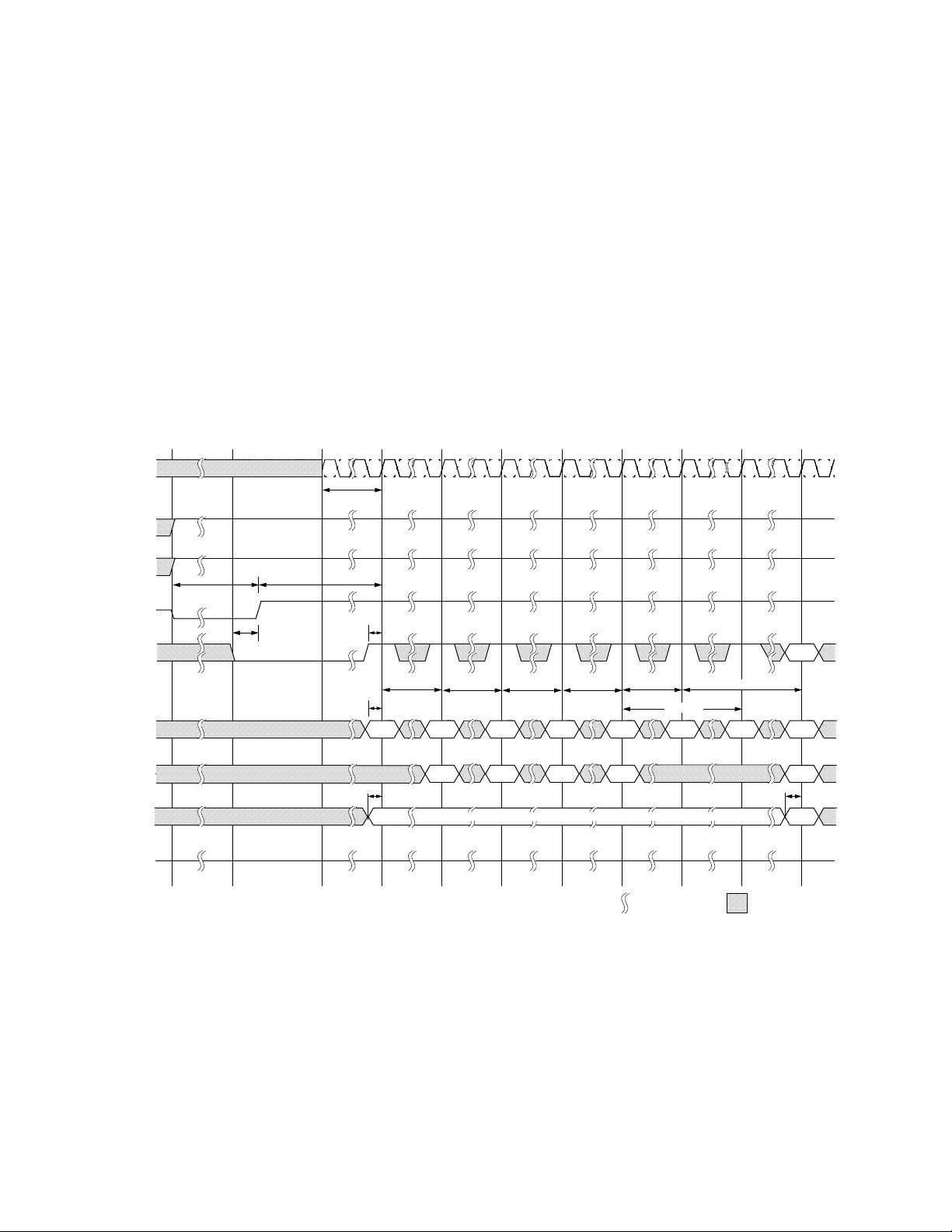
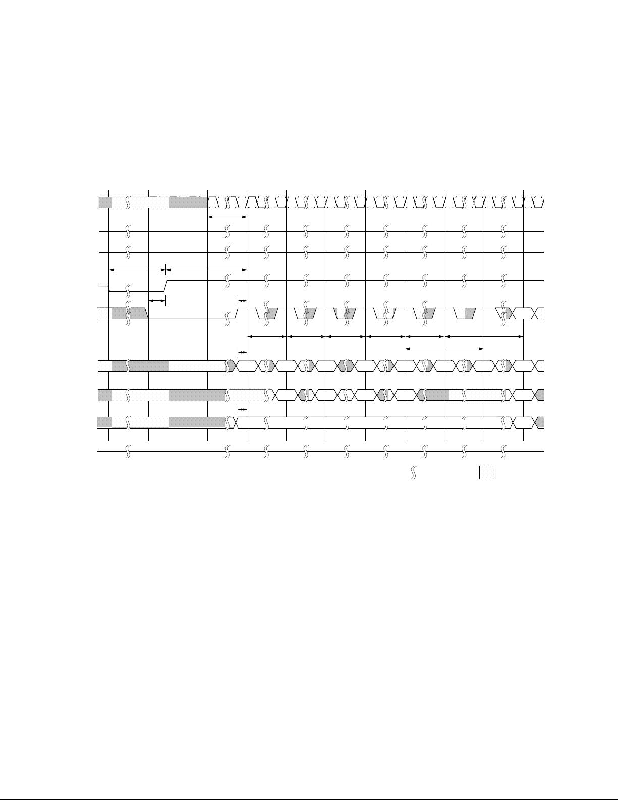
The following sequence is required for POWER UP and Initialization and is shown in Figure 3.
1. Apply power (RESET_n is recommended to be maintained below 0.2 x VDD; all other inputs may be undefined). RESET_n needs
to be maintained for minimum 200us with stable power. CKE is pulled “ Low” anytime before RESET_n being de-asserted (min.
time 10ns) . The power voltage ramp time between 300mV to V
DD
min must be no greater than 200ms; and during the ramp, V
DD
≥ V
DDQ
and (V
DD
-V
DDQ
) < 0.3volts. VPP must ramp at the same time or earlier than VDD and VPP must be equal to or higher
than VDD at all times.
• V
DD
and V
DDQ
are driven from a single power converter output, AND
• The voltage levels on all pins other than V
DD
,V
DDQ
,V
SS
,V
SSQ
must be less than or equal to V
DDQ
and V
DD
on one side and
must be larger than or equal to V
SSQ
and V
SS
on the other side. In addition, V
TT
is limited to TBDV max once power ramp is
finished, AND
• VrefCA tracks TBD.
or
• Apply V
DD
without any slope reversal before or at the same time as V
DDQ
• Apply V
DDQ
without any slope reversal before or at the same time as V
TT
& VrefCA.
• Apply VPP without any slope reversal before or at the same time as VDD.
• The voltage levels on all pins other than V
DD
,V
DDQ
,V
SS
,V
SSQ
must be less than or equal to V
DDQ
and V
DD
on one side and
must be larger than or equal to V
SSQ
and V
SS
on the other side.
2. After RESET_n is de-asserted, wait for another 500us until CKE becomes active. During this time, the DRAM will start internal
initialization; this will be done independently of external clocks.
3. Clocks (CK_t,CK_c) need to be started and stabilized for at least 10ns or 5tCK (which is larger) before CKE goes active. Since
CKE is a synchronous signal, the corresponding setup time to clock (tIS) must be met. Also a Deselect command must be
registered (with tIS set up time to clock) at clock edge Td. Once the CKE registered “High” after Reset, CKE needs to be
continuously registered “High” until the initialization sequence is finished, including expiration of tDLLK and tZQinit
4. The DDR4 SDRAM keeps its on-die termination in high-impedance state as long as RESET_n is asserted. Further, the SDRAM
keeps its on-die termination in high impedance state after RESET_n deassertion until CKE is registered HIGH. The ODT input
signal may be in undefined state until tIS before CKE is registered HIGH. When CKE is registered HIGH, the ODT input signal
may be statically held at either LOW or HIGH. If RTT_NOM is to be enabled in MR1 the ODT input signal must be statically held
LOW. In all cases, the ODT input signal remains static until the power up initialization sequence is finished, including the expiration
of tDLLK and tZQinit.


