没有合适的资源?快使用搜索试试~ 我知道了~
首页I2C-bus specification and user manual.pdf
I2C-Bus 是一种世界范围的标准,使用广泛。通用的I2C总线被使用在各种控制架构之中,如:系统管理总线(SMBus)、电源管理总线(PMBus),智能平台管理接口(IPMI),显示数据通道(DDC)和高级电信计算架构(ATCA)。本文档主要是规范IIC的开发,是学习IIC以及使用IIC的必备参考资料。
资源详情
资源评论
资源推荐
UM10204
I
2
C-bus specification and user manual
Rev. 6 — 4 April 2014 User manual
Document information
Info Content
Keywords I2C, I2C-bus, Standard-mode, Fast-mode, Fast-mode Plus, Fm+,
Ultra Fast-mode, UFm, High Speed, Hs, inter-IC, SDA, SCL, USDA, USCL
Abstract Philips Semiconductors (now NXP Semiconductors) developed a simple
bidirectional 2-wire bus for efficient inter-IC control. This bus is called the
Inter-IC or I
2
C-bus. Only two bus lines are required: a serial data line
(SDA) and a serial clock line (SCL). Serial, 8-bit oriented, bidirectional
data transfers can be made at up to 100 kbit/s in the Standard-mode, up to
400 kbit/s in the Fast-mode, up to 1 Mbit/s in the Fast-mode Plus (Fm+), or
up to 3.4 Mbit/s in the High-speed mode. The Ultra Fast-mode is a
uni-directional mode with data transfers of up to 5 Mbit/s.
UM10204 All information provided in this document is subject to legal disclaimers. © NXP Semiconductors N.V. 2014. All rights reserved.
User manual Rev. 6 — 4 April 2014 2 of 64
Contact information
For more information, please visit: http://www.nxp.com
For sales office addresses, please send an email to: salesaddresses@nxp.com
NXP Semiconductors
UM10204
I
2
C-bus specification and user manual
Revision history
Rev Date Description
v.6 20140404 User manual; sixth release
Modifications: • Figure 41 “R
p(max)
as a function of bus capacitance” updated (recalculated)
• Figure 42 “R
p(min)
as a function of V
DD
” updated (recalculated)
v.5 20121009 User manual; fifth release
v.4 20120213 User manual Rev. 4
v.3 20070619 Many of today’s applications require longer buses and/or faster speeds. Fast-mode Plus was
introduced to meet this need by increasing drive strength by as much as 10× and increasing the
data rate to 1 Mbit/s while maintaining downward compatibility to Fast-mode and Standard-mode
speeds and software commands.
v2.1 2000 Version 2.1 of the I
2
C-bus specification
v2.0 1998 The I
2
C-bus has become a de facto world standard that is now implemented in over 1000 different
ICs and licensed to more than 50 companies. Many of today’s applications, however, require higher
bus speeds and lower supply voltages. This updated version of the I
2
C-bus specification meets those
requirements.
v1.0 1992 Version 1.0 of the I
2
C-bus specification
Original 1982 first release
UM10204 All information provided in this document is subject to legal disclaimers. © NXP Semiconductors N.V. 2014. All rights reserved.
User manual Rev. 6 — 4 April 2014 3 of 64
NXP Semiconductors
UM10204
I
2
C-bus specification and user manual
1. Introduction
The I
2
C-bus is a de facto world standard that is now implemented in over 1000 different
ICs manufactured by more than 50 companies. Additionally, the versatile I
2
C-bus is used
in various control architectures such as System Management Bus (SMBus), Power
Management Bus (PMBus), Intelligent Platform Management Interface (IPMI), Display
Data Channel (DDC) and Advanced Telecom Computing Architecture (ATCA).
This document assists device and system designers to understand how the I
2
C-bus works
and implement a working application. Various operating modes are described. It contains
a comprehensive introduction to the I
2
C-bus data transfer, handshaking and bus
arbitration schemes. Detailed sections cover the timing and electrical specifications for the
I
2
C-bus in each of its operating modes.
Designers of I
2
C-compatible chips should use this document as a reference and ensure
that new devices meet all limits specified in this document. Designers of systems that
include I
2
C devices should review this document and also refer to individual component
data sheets.
2. I
2
C-bus features
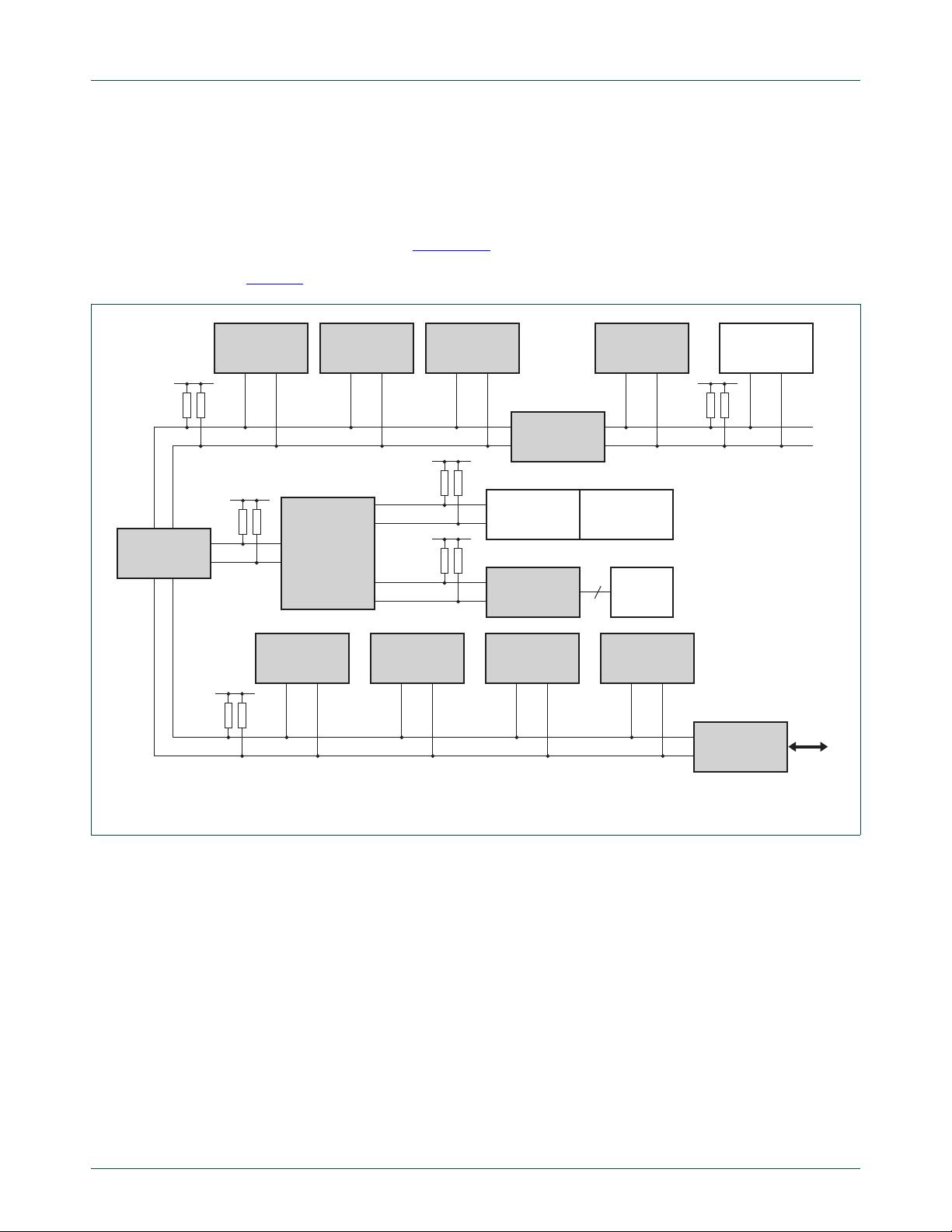
In consumer electronics, telecommunications and industrial electronics, there are often
many similarities between seemingly unrelated designs. For example, nearly every
system includes:
• Some intelligent control, usually a single-chip microcontroller
• General-purpose circuits like LCD and LED drivers, remote I/O ports, RAM,
EEPROM, real-time clocks or A/D and D/A converters
• Application-oriented circuits such as digital tuning and signal processing circuits for
radio and video systems, temperature sensors, and smart cards
To exploit these similarities to the benefit of both systems designers and equipment
manufacturers, as well as to maximize hardware efficiency and circuit simplicity, Philips
Semiconductors (now NXP Semiconductors) developed a simple bidirectional 2-wire bus
for efficient inter-IC control. This bus is called the Inter IC or I
2
C-bus. All I
2
C-bus
compatible devices incorporate an on-chip interface which allows them to communicate
directly with each other via the I
2
C-bus. This design concept solves the many interfacing
problems encountered when designing digital control circuits.
Here are some of the features of the I
2
C-bus:
• Only two bus lines are required; a serial data line (SDA) and a serial clock line (SCL).
• Each device connected to the bus is software addressable by a unique address and
simple master/slave relationships exist at all times; masters can operate as
master-transmitters or as master-receivers.
• It is a true multi-master bus including collision detection and arbitration to prevent data
corruption if two or more masters simultaneously initiate data transfer.
• Serial, 8-bit oriented, bidirectional data transfers can be made at up to 100 kbit/s in
the Standard-mode, up to 400 kbit/s in the Fast-mode, up to 1 Mbit/s in Fast-mode
Plus, or up to 3.4 Mbit/s in the High-speed mode.
碰撞检测与仲裁
UM10204 All information provided in this document is subject to legal disclaimers. © NXP Semiconductors N.V. 2014. All rights reserved.
User manual Rev. 6 — 4 April 2014 4 of 64
NXP Semiconductors
UM10204
I
2
C-bus specification and user manual
• Serial, 8-bit oriented, unidirectional data transfers up to 5 Mbit/s in Ultra Fast-mode
• On-chip filtering rejects spikes on the bus data line to preserve data integrity.
• The number of ICs that can be connected to the same bus is limited only by a
maximum bus capacitance. More capacitance may be allowed under some
conditions. Refer to Section 7.2
.
Figure 1
shows an example of I
2
C-bus applications.
2.1 Designer benefits
I
2
C-bus compatible ICs allow a system design to progress rapidly directly from a
functional block diagram to a prototype. Moreover, since they ‘clip’ directly onto the
I
2
C-bus without any additional external interfacing, they allow a prototype system to be
modified or upgraded simply by ‘clipping’ or ‘unclipping’ ICs to or from the bus.
Here are some of the features of I
2
C-bus compatible ICs that are particularly attractive to
designers:
• Functional blocks on the block diagram correspond with the actual ICs; designs
proceed rapidly from block diagram to final schematic.
• No need to design bus interfaces because the I
2
C-bus interface is already integrated
on-chip.
Fig 1. Example of I
2
C-bus applications
I
2
C
A/D or D/A
Converters
I
2
C
General Purpose
I/O Expanders
I
2
C
LED Controllers
V
DD4
I
2
C
Repeaters/
Hubs/Extenders
I
2
C
DIP Switches
V
DD5
I
2
C
Slave
V
DD0
V
DD1
PCA9541
I
2
C
Master Selector/
Demux
I
2
C
Multiplexers
and Switches
V
DD2
I
2
C Port
via HW or
Bit Banging
I
2
C
Bus Controllers
MCUs
8
MCUs
I
2
C
Serial EEPROMs
LCD Drivers
(with I
2
C)
I
2
C
Real Time Clock/
Calendars
V
DD3
I
2
C
Temperature
Sensors
Bridges
(with I
2
C)
SPI
UART
USB
002aac858
UM10204 All information provided in this document is subject to legal disclaimers. © NXP Semiconductors N.V. 2014. All rights reserved.
User manual Rev. 6 — 4 April 2014 5 of 64
NXP Semiconductors
UM10204
I
2
C-bus specification and user manual
• Integrated addressing and data-transfer protocol allow systems to be completely
software-defined.
• The same IC types can often be used in many different applications.
• Design-time reduces as designers quickly become familiar with the frequently used
functional blocks represented by I
2
C-bus compatible ICs.
• ICs can be added to or removed from a system without affecting any other circuits on
the bus.
• Fault diagnosis and debugging are simple; malfunctions can be immediately traced.
• Software development time can be reduced by assembling a library of reusable
software modules.
In addition to these advantages, the CMOS ICs in the I
2
C-bus compatible range offer
designers special features which are particularly attractive for portable equipment and
battery-backed systems.
They all have:
• Extremely low current consumption
• High noise immunity
• Wide supply voltage range
• Wide operating temperature range.
2.2 Manufacturer benefits
I
2
C-bus compatible ICs not only assist designers, they also give a wide range of benefits
to equipment manufacturers because:
• The simple 2-wire serial I
2
C-bus minimizes interconnections so ICs have fewer pins
and there are not so many PCB tracks; result — smaller and less expensive PCBs.
• The completely integrated I
2
C-bus protocol eliminates the need for address decoders
and other ‘glue logic’.
• The multi-master capability of the I
2
C-bus allows rapid testing and alignment of
end-user equipment via external connections to an assembly line.
• The availability of I
2
C-bus compatible ICs in various leadless packages reduces
space requirements even more.
These are just some of the benefits. In addition, I
2
C-bus compatible ICs increase system
design flexibility by allowing simple construction of equipment variants and easy
upgrading to keep designs up-to-date. In this way, an entire family of equipment can be
developed around a basic model. Upgrades for new equipment, or enhanced-feature
models (that is, extended memory, remote control, etc.) can then be produced simply by
clipping the appropriate ICs onto the bus. If a larger ROM is needed, it is simply a matter
of selecting a microcontroller with a larger ROM from our comprehensive range. As new
ICs supersede older ones, it is easy to add new features to equipment or to increase its
performance by simply unclipping the outdated IC from the bus and clipping on its
successor.
剩余63页未读,继续阅读
Akun93
- 粉丝: 8
- 资源: 3
上传资源 快速赚钱
- 我的内容管理 收起
- 我的资源 快来上传第一个资源
- 我的收益 登录查看自己的收益
- 我的积分 登录查看自己的积分
- 我的C币 登录后查看C币余额
- 我的收藏
- 我的下载
- 下载帮助
会员权益专享
最新资源
- 27页智慧街道信息化建设综合解决方案.pptx
- 计算机二级Ms-Office选择题汇总.doc
- 单链表的插入和删除实验报告 (2).docx
- 单链表的插入和删除实验报告.pdf
- 物联网智能终端项目设备管理方案.pdf
- 如何打造品牌的模式.doc
- 样式控制与页面布局.pdf
- 武汉理工Java实验报告(二).docx
- 2021线上新品消费趋势报告.pdf
- 第3章 Matlab中的矩阵及其运算.docx
- 基于Web的人力资源管理系统的必要性和可行性.doc
- 基于一阶倒立摆的matlab仿真实验.doc
- 速运公司物流管理模式研究教材
- 大数据与管理.pptx
- 单片机课程设计之步进电机.doc
- 大数据与数据挖掘.pptx
资源上传下载、课程学习等过程中有任何疑问或建议,欢迎提出宝贵意见哦~我们会及时处理!
点击此处反馈
安全验证
文档复制为VIP权益,开通VIP直接复制
信息提交成功
评论0