
Rev 0.4 / Jun. 2007 4
HY27UF(08/16)1G2A Series
1Gbit (128Mx8bit / 64Mx16bit) NAND Flash
1. SUMMARY DESCRIPTION
The Hynix HY27UF(08/16)1G2A series is a 128Mx8bit with spare 4Mx8 bit capacity. The device is offered in 3.3V Vcc
Power Supply.
Its NAND cell provides the most cost-effective solution for the solid state mass storage market. The memory is divided
into blocks that can be erased independently so it is possible to preserve valid data while old data is erased.
The device contains 1024 blocks, composed by 64 pages consisting in two NAND structures of 32 series connected
Flash cells.
A program operation allows to write the 2112-byte page in typical 200us and an erase operation can be performed in
typical 2ms on a 128K-byte(X8 device) block.
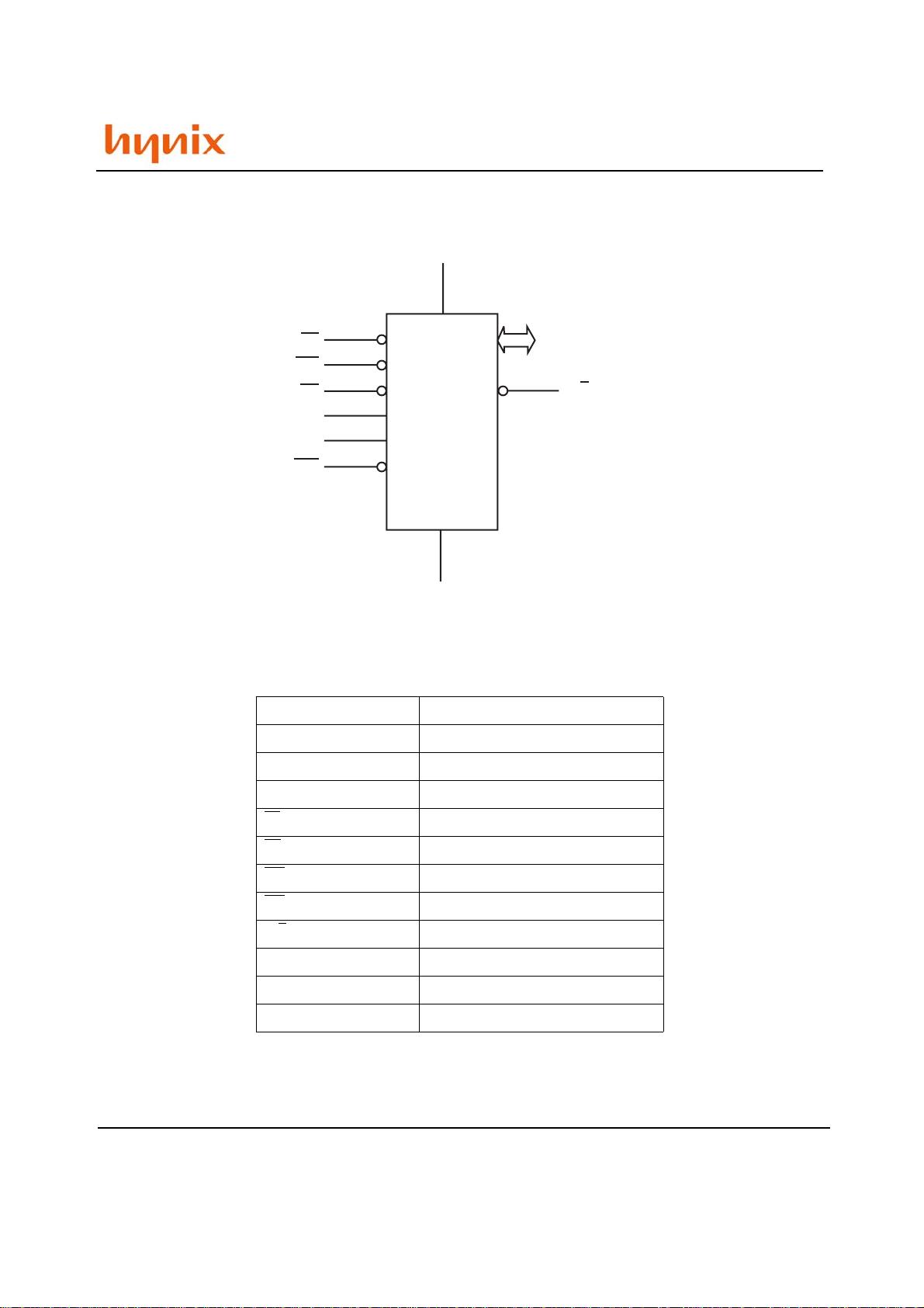
Data in the page can be read out at 30ns cycle time per byte. The I/O pins serve as the ports for address and data
input/output as well as command input. This interface allows a reduced pin count and easy migration towards different
densities, without any rearrangement of footprint.
Commands, Data and Addresses are synchronously introduced using CE
, WE, ALE and CLE input pin. The on-chip Pro-
gram/Erase Controller automates all program and erase functions including pulse repetition, where required, and inter-
nal verification and margining of data.
The modify operations can be locked using the WP
input pin or using the extended lock block feature described later.
The output pin R/B
(open drain buffer) signals the status of the device during each operation. In a system with multi-
ple memories the R/B pins can be connected all together to provide a global status signal.
Even the write-intensive systems can take advantage of the HY27UF(08/16)1G2A extended reliability of 100K pro-
gram/erase cycles by providing ECC (Error Correcting Code) with real time mapping-out algorithm.
The chip could be offered with the CE
don’t care function. This function allows the direct download of the code from
the NAND Flash memory device by a microcontroller, since the CE
transitions do not stop the read operation.
The copy back function allows the optimization of defective blocks management: when a page program operation fails
the data can be directly programmed in another page inside the same array section without the time consuming serial
data insertion phase.
The cache program feature allows the data insertion in the cache register while the data register is copied into the
flash array. This pipelined program operation improves the program throughput when long files are written inside the
memory. A cache read feature is also implemented. This feature allows to dramatically improve the read throughput
when consecutive pages have to be streamed out.
The HYNIX HY27UF(08/16)1G2A series is available in 48 - TSOP1 12 x 20 mm, 48 - USOP 12 x 17 mmm, FBGA 9 x
11 mm.
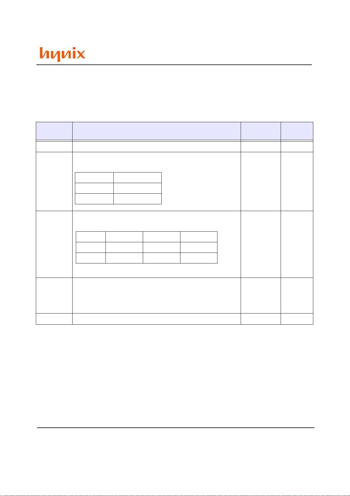
1.1 Product List
PART NUMBER ORIZATION VCC RANGE PACKAGE
HY27UF081G2A x8
2.7V - 3.6 Volt
63FBGA / 48TSOP1 / 48USOP1
HY27UF161G2A x16 48TSOP1


 我的内容管理
收起
我的内容管理
收起
 我的收益 登录查看自己的收益
 我的积分
登录查看自己的积分
我的积分
登录查看自己的积分
 我的C币
登录后查看C币余额
我的C币
登录后查看C币余额
 我的收藏
我的收藏  我的下载
我的下载  下载帮助
下载帮助 


评论1