没有合适的资源?快使用搜索试试~ 我知道了~
首页AD9361射频和基带锁相环用户手册.pdf
AD9361射频和基带锁相环用户手册.pdf
需积分: 41 915 浏览量
更新于2023-05-24
评论 1
收藏 1.77MB PDF 举报
AD9361是一款面向3G和4G基站应用的高性能、高集成度的射频(RF)Agile Transceiver™捷变收发器。该器件的可编程性和宽带能力使其成为多种收发器应用的理想选择。该器件集RF前端与灵活的混合信号基带部分为一体,集成频率合成器,为处理器提供可配置数字接口,从而简化设计导入。AD9361接收器LO工作频率范围为70 MHz至6.0 GHz,发射器LO工作频率范围为47 MHz至6.0 GHz,涵盖大部分特许执照和免执照频段,支持的通道带宽范围为200 kHz以下至56 MHz。
资源详情
资源评论
资源推荐

AD9361
RF and BB PLL Synthesizer
User Guide

ADI Confidential
AD9361 RF and BB PLL Synthesizer User Guide
Rev 2.4.
Information furnished by Analog Devices is believed to be accurate and reliable. However, no
responsibility is assumed by Analog Devices for its use, nor for any infringements of patents or other
rights of third parties that may result from its use. Specifications subject to change without notice. No
license is granted by implication or otherwise under any patent or patent rights of Analog Devices.
Trademarks and registered trademarks are the property of their respective owners.
One Technology Way, P.O. Box 9106, Norwood, MA 02062-9106, U.S.A.
Tel: 781.329.4700
www.analog.com
Fax: 781.461.3113 ©2010 Analog Devices, Inc. All rights reserved.
GENERAL DESCRIPTION
The AD9361 transceiver contains two identical RFPLL synthesizers to generate the required LO signals. One is programmed for the RX
channel and the other for the TX channel. The transceiver also contains a BBPLL synthesizer to generate the required sampling and
internal operational clocks. The PLL synthesizers are all of fractional–N architecture with completely integrated VCOs and loop filters.
They require no external parts to cover the entire frequency range of the device. This configuration allows the use of any convenient
reference frequency for operation on any channel with any sample rate. For FDD operation, the frequency of TX and RX can be different
and both RFPLL synthesizers operate simultaneously. For TDD operation, the RFPLL synthesizers alternately turn on as appropriate for
RX and TX frames.
REVISION HISTORY
3/11—1.0 Distribution
4/11—1.1 Edit formatting add table. Applies to R1 version.
6/11—2.0 Update fixed writes for R2. Add Fast Lock info, Ext LO.
9/11—2.1 Include FDD and TDD tables for R2. Add BBPLL section. Examples updated.
10/11—2.2 Fixed typos.
11/11—2.3 Clarified BBPLL loop filter table value usage
1/12—2.4 Added how to generate TDD script with FDD calibrations to TDD MODE – Faster Lock Times section.

ADI Confidential
AD9361 RF and BB PLL Synthesizer User Guide
Page 3 of 47
TABLE OF CONTENTS
General Description ........................................................................................................................................................................................................... 2
Revision History ................................................................................................................................................................................................................. 2
RFPLL Introduction ........................................................................................................................................................................................................... 4
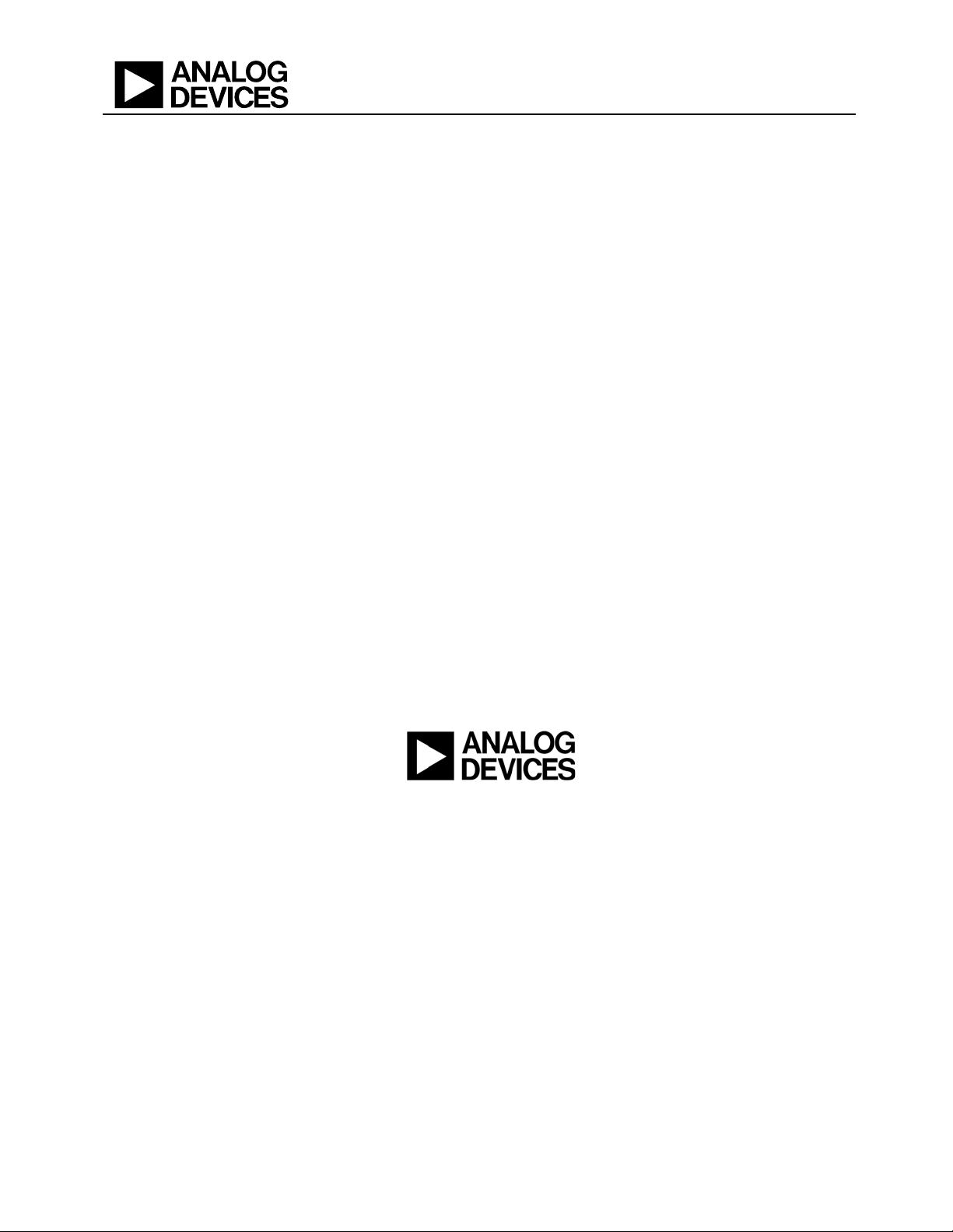
AD9361 PLL Architecture................................................................................................................................................................................................. 5
Reference Block (including Reference Scalers) ................................................................................................................................................................ 5
DCXO .............................................................................................................................................................................................................................. 6
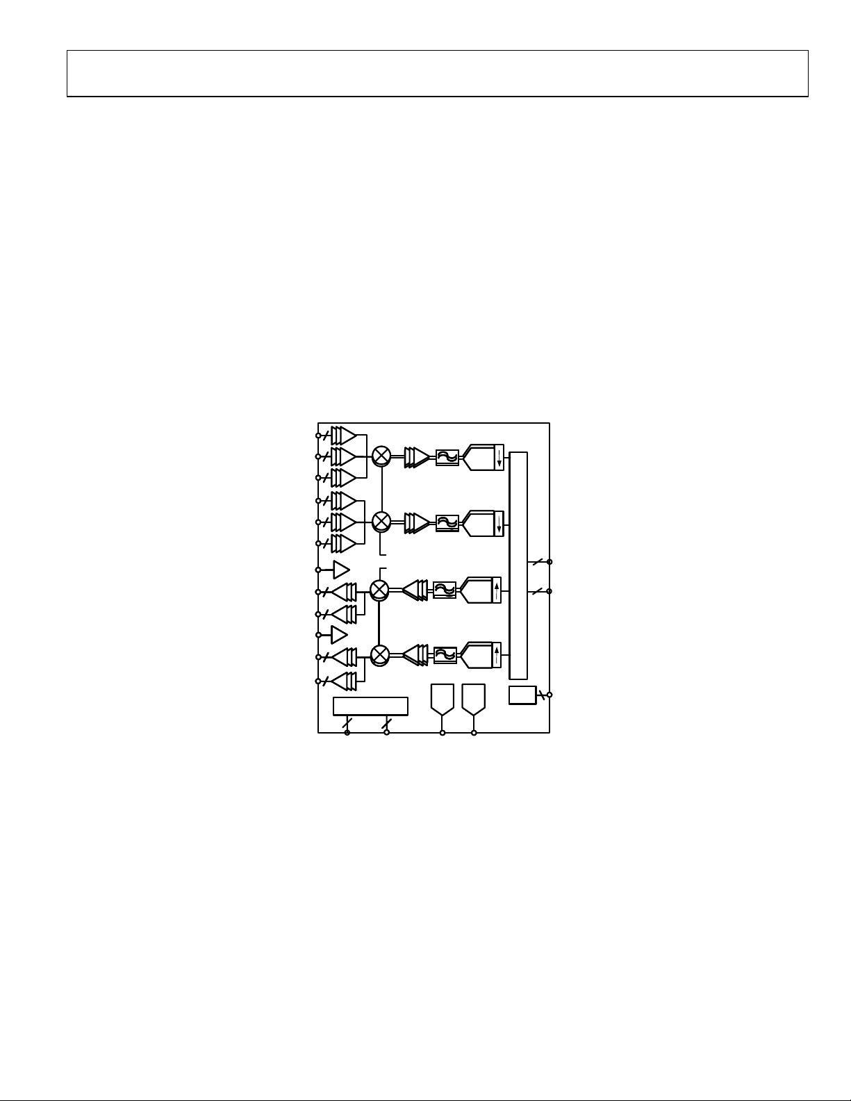
Main PLL Block .................................................................................................................................................................................................................. 6
VCO Divider Block ........................................................................................................................................................................................................ 7
Calculating RFPLL Divider Values .................................................................................................................................................................................. 7
Carrier Frequency setup ................................................................................................................................................................................................ 7
RX (or TX) VCO Divider.............................................................................................................................................................................................. 7
Charge Pump Current ....................................................................................................................................................................................................... 9
RFPLL Loop Filter ............................................................................................................................................................................................................ 10
VCO Configuration ......................................................................................................................................................................................................... 10
Lock Detector ................................................................................................................................................................................................................... 11
Synthesizer Look Up Table .............................................................................................................................................................................................. 11
Example Programming Sequence .................................................................................................................................................................................. 26
TDD MODE – Faster Lock Times ................................................................................................................................................................................. 28
Frequency Correction Words ......................................................................................................................................................................................... 29
FastLock Mode ................................................................................................................................................................................................................. 30
FastLock Initial Wider-BW Option ........................................................................................................................................................................... 30
Configuring and Using a Fast Lock Profile – Internal Registers ........................................................................................................................... 31
Configuring and Using a Fast Lock Profile – EXAMPLE ...................................................................................................................................... 34
External LO ....................................................................................................................................................................................................................... 37
Baseband PLL (BBPLL) ................................................................................................................................................................................................... 39
BBPLL VCO ...................................................................................................................................................................................................................... 39
Calculating BBPLL Divider Values ................................................................................................................................................................................ 40
BB PLL Charge Pump ...................................................................................................................................................................................................... 41
BBPLL Loop Filter Values ............................................................................................................................................................................................... 41
BBPLL Typical Loop Filter and Charge Pump Configuration ................................................................................................................................... 44
APPENDIX: RFPLL Loop Filter ................................................................................................................................................................................... 45

ADI Confidential
AD9361 RF and BB PLL Synthesizer User Guide
Page 4 of 47
RFPLL INTRODUCTION
The AD9361 contains two identical RFPLL Synthesizers, one for RX and the other for TX, which are programmed independently. The
two VCOs and loop filters are integrated on chip and have no external components. The fundamental frequency of the PLLs is from 6-
12GHz. Local Oscillator frequencies ranging from 47MHz to 6GHz are created by dividing the PLL frequency.
There are 6 areas of each PLL that will be configured for a given frequency of operation. These are:
• Reference Scaler
• PLL divider (N
INT
and N
FRAC
) (register bits)
• VCO divider (register bits)
• Charge Pump (register bits)
• Loop Filter components (register bits)
• VCO tuning (self-calibration procedure)
RX 1A
AD9361
DAC
DAC
DAC
DAC
TX2A
DAC
DAC
DAC
DAC
TX1A
GPO
ADC
DAC
RADIO
AUXADC
CTRL
CTRL
GPO
ADC
DAC
RADIO
SWITCHING
CTRL
CTRL
TX2B
TX1B
RX 1C
RX 2A
RX 2C
SPI Port
D
a
t
a
I
n
t
e
r
f
a
c
e
AUXDAC
JESD207/
LVDS
Rx Synth
Tx Synth
RX 2B
RX 1B
JESD207/
LVDS
DAC
DACDAC
ADC
DAC
DAC
DAC
ADC
Tx Monitor 1
Tx Monitor 2
Figure 1. AD9361 Block Diagram. RX and TX synthesizers operate independently.
The synthesizers have identical but independent register sets in the device address space. Each synthesizer must be configured and
calibrated separately.
ADI provides Lookup Tables for synthesizer configuration based upon the desired reference frequency to be used. Each lookup table
covers a specific reference clock input frequency and application (FDD or TDD). A particular lookup table is indexed by the VCO
frequency. At that index, the configuration data in the table cells is retrieved, then it is formatted and stored into the appropriate
registers. At power up, a few registers are programmed that will typically remain the same during normal operation. At this point, a
particular table is referenced to configure the VCO and loop filter settings for best performance over temperature. The tables provided by
ADI include a column of VCO gains for different frequency settings so that users can customize their own loop filter if desired.

ADI Confidential
AD9361 RF and BB PLL Synthesizer User Guide
Page 5 of 47
AD9361 PLL ARCHITECTURE
The following sections show block diagrams of the AD9361 PLL that consist of the Reference Block, the main PLL Block, and the LO
GEN Output Block. The VCO always operates between 6 to 12 GHz. Highlighted text indicates programmable items.
REFERENCE BLOCK (including Reference Scalers)
The reference frequency can be generated via the on-chip DCXO or an external clock source can provide this input to the device. If an
external source is used, a 1.3Vpp clipped sinewave would be applied to the device XTAL_N input (with XTAL_P input OPEN). A MUX
selects the desired source. The reference is then split and applied to 3 independent conditioning blocks also known as scalers (or Ref
Dividers in the Register Map). The conditioning blocks provide 4 options such that the PLL reference frequency F
REF
(the loop reference
applied to the PLL phase detector) is either buffered, doubled, halved, or divided by 4. Independent blocks make it possible to have a
different F
REF
for each PLL if desired. For best RFPLL performance, ADI recommends selecting the reference scaler that will result in a
reference frequency as high as possible with the result between 35MHz and 80 MHz after scaling. Also, the same scaler configuration
should be used for both RX and TX PLLs so that the noise spectrums match. The same block functionality is provided for the BBPLL (see
BBPLL section). For best BBPLL performance, the reference scaler would be configured to result in reference frequencies between 35 and
70MHz. See Table 1 for configuration information.
Figure 2. Independent Reference Block for each PLL applies either Buffered, 2X, ½X, or ¼X Reference Frequency
For best performance, Vali d F
REF
for TX and RX is 35-80MHz
NOTE: Apply External Reference to the XTAL_N pin (XTAL_P OPEN)
(DO NOT APPLY TO REF_CLK_IN pin). See DCXO document.
RX REFCLK Scale {0x2AB[0], 0x2AC[7]} TX REFCLK Scale 0x2AC[3:2] BB REFCLK Scale 0x045[1:0]
1 00 1 00 1 00
½ 01 ½ 01 ½ 01
¼ 10 ¼ 10 ¼ 10
2 11 2 11 2 11
Table 1 Reference Block Scaler Configuration
RX Ref Divider
[1:0]
H
6
REF
_
CLK
_
IN
DO NOT USE
DCXO
20
-
50
MHz
TX Ref Divider
BBPLL Ref Divider
M
11
M
12
XTALN OR
EXTERNAL REFERENCE INPUT
5 - 320MHz (19-80MHz Recommended)
1
0
XO Bypass
0
x
009
[
4
]
1
0
DCXO Enable
Ref Pad
Power Down
(
Set to
1
)
0
x
2
AB
[
2
]
BBPLL
F
REF
TX SYNTH
F
REF
10
–
80
MHz
RX SYNTH
F
REF
10
–
80
MHz
/2
/4
x2
/2
/4
x2
/2
/4
x2
0
x
009
[
1
]
FOR BEST
PERFORMANCE:
35-70 MHz
FOR BEST
PERFORMANCE:
35-80MHz
XTALP OR
OPEN for EXTERNAL REFERENCE
[1:0]
[1:0]
CONNECT H6 TO GROUND
剩余46页未读,继续阅读


安全验证
文档复制为VIP权益,开通VIP直接复制

评论0