Contents
State Diagram .................................................................................................................................................. 9
Functional Description ................................................................................................................................... 10
Industrial Temperature .............................................................................................................................. 10
Automotive Temperature ........................................................................................................................... 11
General Notes ............................................................................................................................................ 11
Functional Block Diagrams ............................................................................................................................. 12
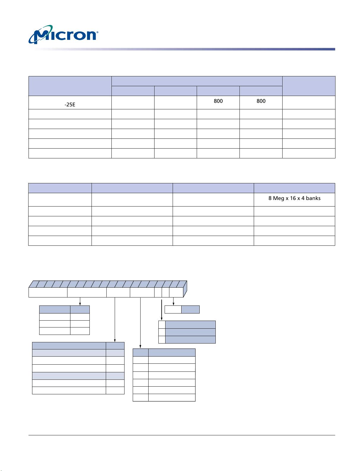
Ball Assignments and Descriptions ................................................................................................................. 15
Packaging ...................................................................................................................................................... 20
Package Dimensions .................................................................................................................................. 20
FBGA Package Capacitance ......................................................................................................................... 26
Electrical Specifications – Absolute Ratings ..................................................................................................... 27
Temperature and Thermal Impedance ........................................................................................................ 27
Electrical Specifications – Idd Parameters ........................................................................................................ 30
Idd Specifications and Conditions ............................................................................................................... 30
Idd7 Conditions ......................................................................................................................................... 31
AC Timing Operating Specifications ................................................................................................................ 35
AC and DC Operating Conditions .................................................................................................................... 46
ODT DC Electrical Characteristics ................................................................................................................... 47
Input Electrical Characteristics and Operating Conditions ............................................................................... 48
Output Electrical Characteristics and Operating Conditions ............................................................................. 51
Output Driver Characteristics ......................................................................................................................... 53
Power and Ground Clamp Characteristics ....................................................................................................... 57
AC Overshoot/Undershoot Specification ......................................................................................................... 58
Input Slew Rate Derating ................................................................................................................................ 60
Commands .................................................................................................................................................... 74
Truth Tables ............................................................................................................................................... 74
DESELECT ................................................................................................................................................. 78
NO OPERATION (NOP) .............................................................................................................................. 79
LOAD MODE (LM) ..................................................................................................................................... 79
ACTIVATE .................................................................................................................................................. 79
READ ......................................................................................................................................................... 79
WRITE ....................................................................................................................................................... 79
PRECHARGE .............................................................................................................................................. 80
REFRESH ................................................................................................................................................... 80
SELF REFRESH ........................................................................................................................................... 80
Mode Register (MR) ........................................................................................................................................ 80
Burst Length .............................................................................................................................................. 81
Burst Type ................................................................................................................................................. 81
Operating Mode ......................................................................................................................................... 83
DLL RESET ................................................................................................................................................. 83
Write Recovery ........................................................................................................................................... 84
Power-Down Mode .................................................................................................................................... 84
CAS Latency (CL) ........................................................................................................................................ 85
Extended Mode Register (EMR) ....................................................................................................................... 86
DLL Enable/Disable ................................................................................................................................... 87
Output Drive Strength ................................................................................................................................ 87
DQS# Enable/Disable ................................................................................................................................. 87
RDQS Enable/Disable ................................................................................................................................. 87
Output Enable/Disable ............................................................................................................................... 87
On-Die Termination (ODT) ........................................................................................................................ 88
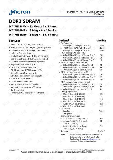
512Mb: x4, x8, x16 DDR2 SDRAM
PDF: 09005aef82f1e6e2
Rev. M 9/08 EN
4
Micron Technology, Inc. reserves the right to change products or specifications without notice.
© 2004 Micron Technology, Inc. All rights reserved.


 我的内容管理
收起
我的内容管理
收起
 我的收益 登录查看自己的收益
 我的积分
登录查看自己的积分
我的积分
登录查看自己的积分
 我的C币
登录后查看C币余额
我的C币
登录后查看C币余额
 我的收藏
我的收藏  我的下载
我的下载  下载帮助
下载帮助 


评论11