没有合适的资源?快使用搜索试试~ 我知道了~
首页Razavi 拉扎维 CMOS IC design 入门经典 Fundamentals_of_Microelectronics02
入门经典 适合CMOS IC design 新手,一般学过电路分析应该看得懂,看完整本书,在接着看拉扎维 另外Design of Analog CMOS Integrated Circuits,应该就没问题了
资源详情
资源评论
资源推荐
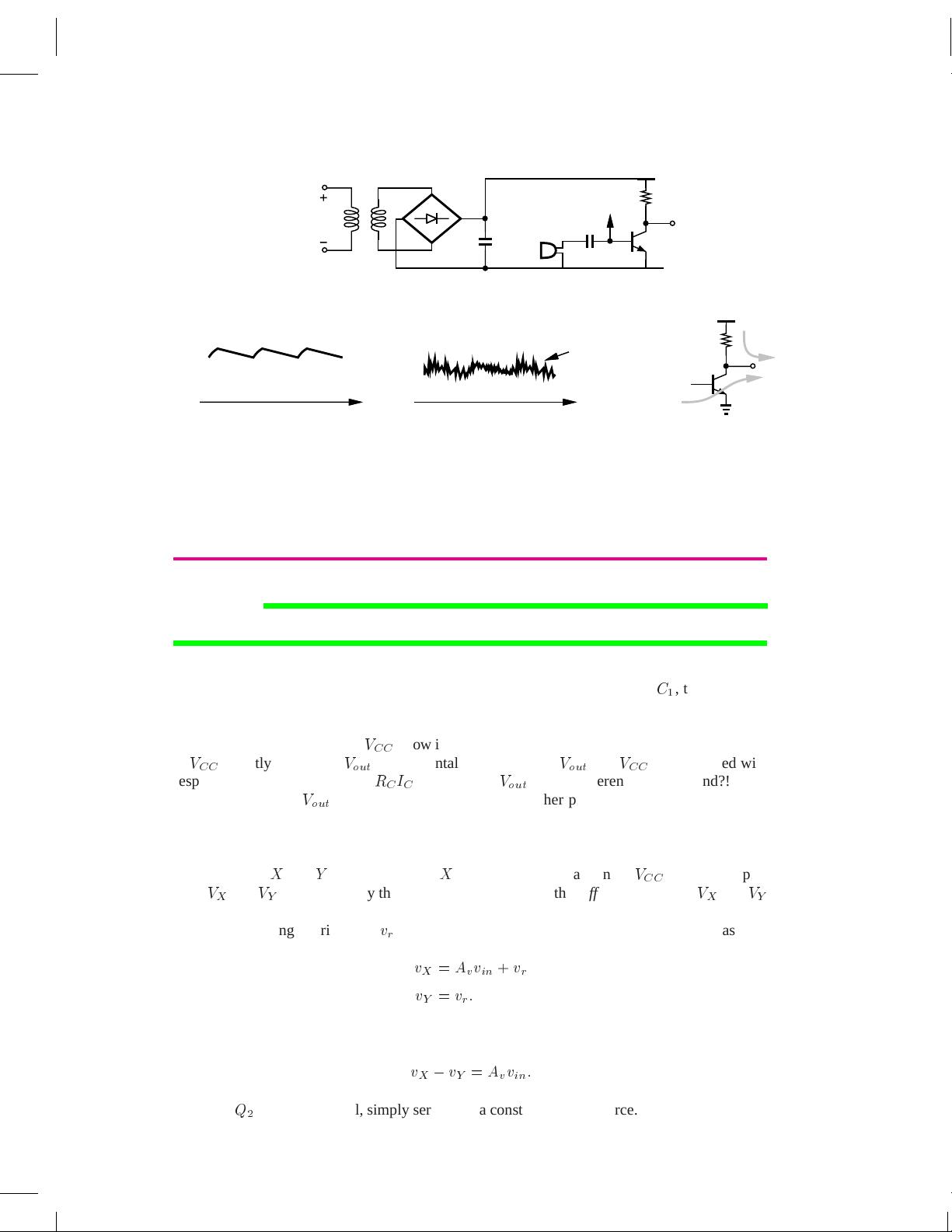
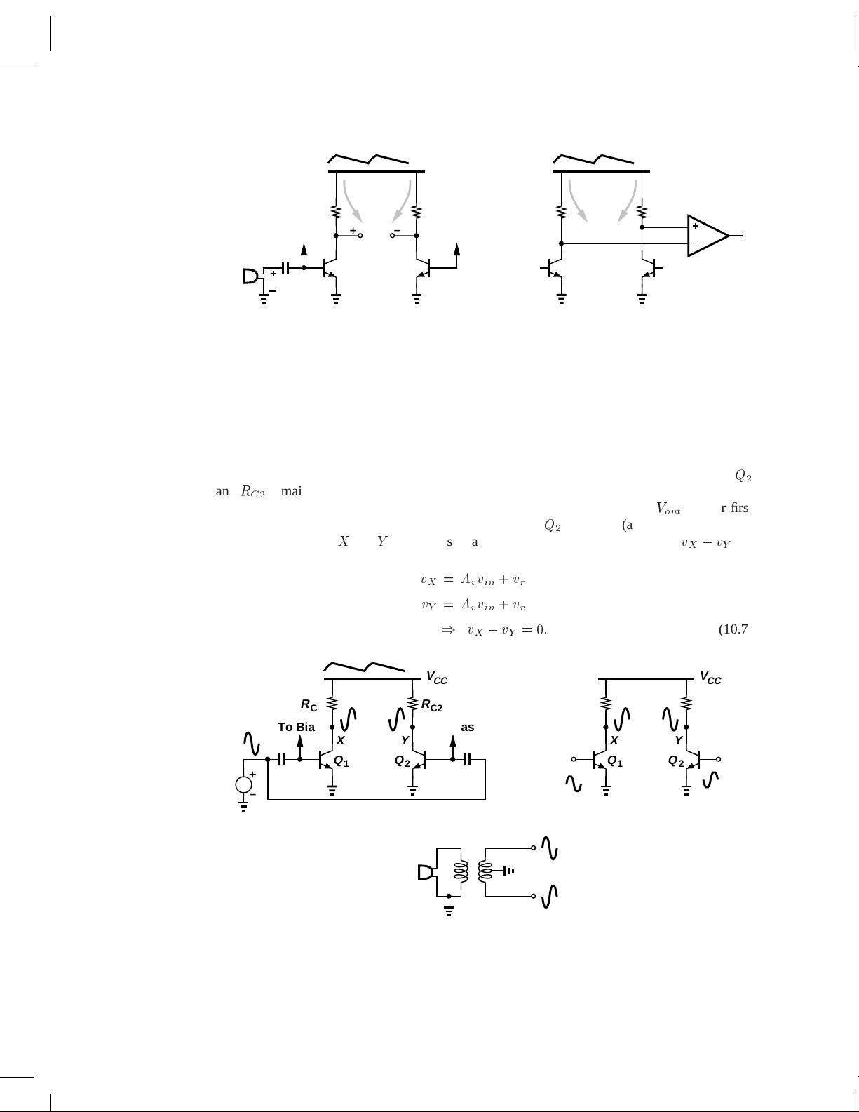
BR Wiley/Razavi/Fundamentals of Microelectronics [Razavi.cls v. 2006] June 30, 2007 at 13:42 466 (1)
10
Differential Amplifiers
The elegant concept of “differential” signals and amplifiers was invented in the 1940s and first
utilized in vacuum-tube circuits. Since then, differential circuits have found increasingly wider
usage in microelectronics and serve as a robust, high-performance design paradigm in many of
today’s systems. This chapter describes bipolar and MOS differential amplifiers and formulates
their large-signal and small-signal properties. The concepts are outlined below.
General
Considerations
Differential Signals
Differential Pair
Bipolar
Differential pair
Qualitative Analysis
Large−Signal Analysis
Small−Signal Analysis
Differential pair
Qualitative Analysis
Large−Signal Analysis
Small−Signal Analysis
MOS
Other Concepts
Cascode Pair
Common−Mode Rejection
Pair with Active Load
10.1 General Considerations
10.1.1 Initial Thoughts
In order to understand the need for differential circuits, let us first consider an example.
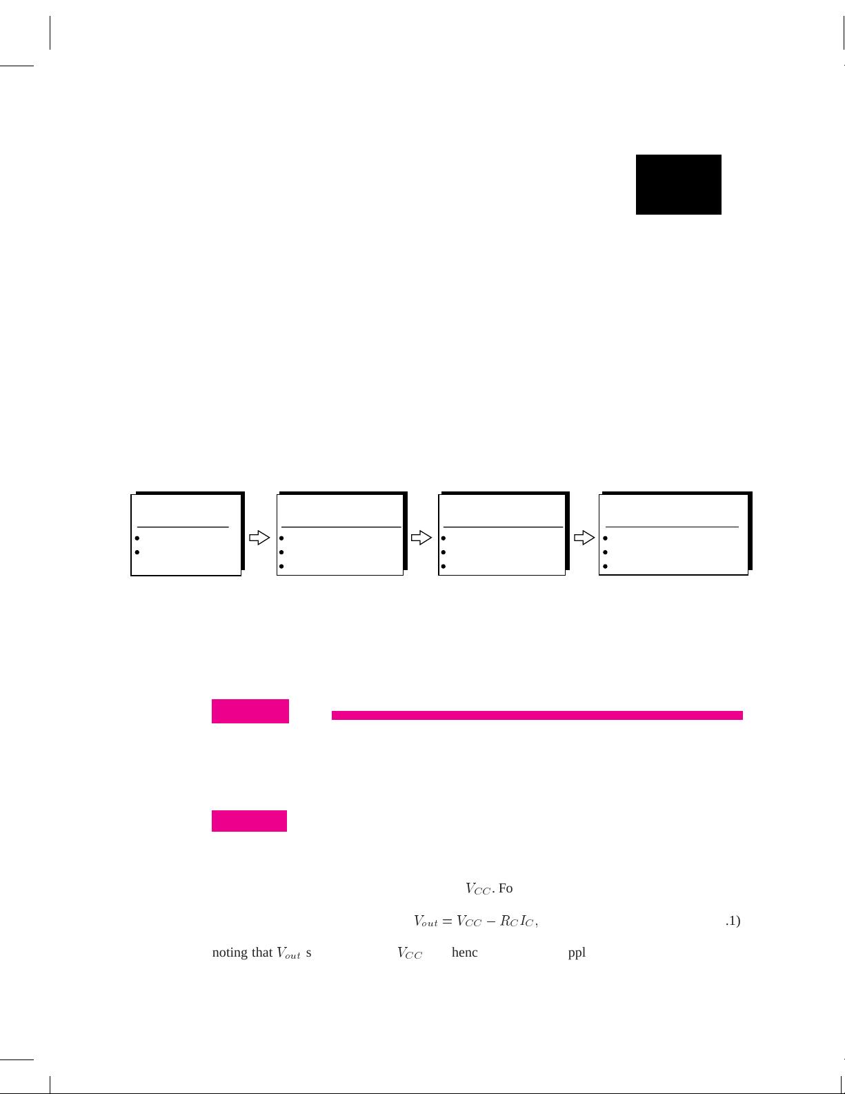
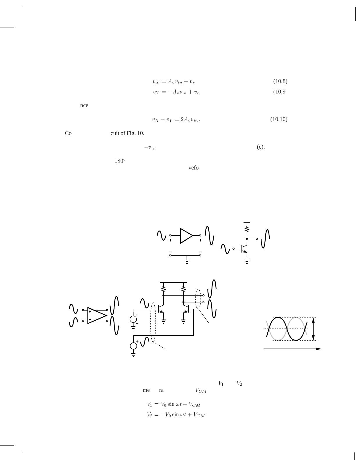
Example 10.1
Having learned the design of rectifiers and basic amplifier stages, an electrical engineering
student constructs the circuit shown in Fig. 10.1(a) to amplify the signal produced by a
microphone. Unfortunately, upon applying the result to a speaker, the student observes that the
amplifier output contains a strong “humming” noise, i.e., a steady low-frequency component.
Explain what happens.
Solution
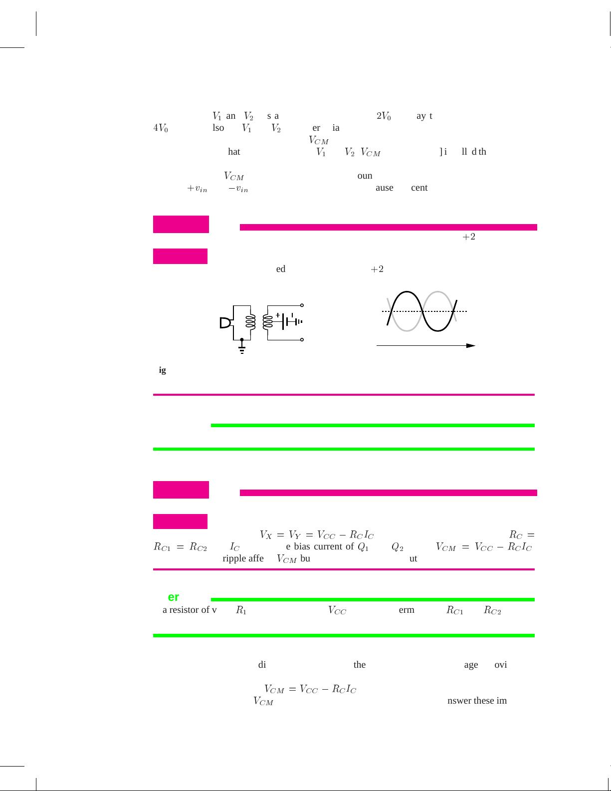
Recall from Chapter 3 that the current drawn from the rectified output creates a ripple waveform
at twice the ac line frequency (50 or 60 Hz) [Fig. 10.1(b)]. Examining the output of the common-
emitter stage, we can identify two components: (1) the amplified version of the microphone
signal and (2) the ripple waveform present on
V
CC
. For the latter, we can write
V
out
=
V
CC
,
R
C
I
C
;
(10.1)
noting that
V
out
simply “tracks”
V
CC
and hence contains the ripple in its entirety. The “hum”
originates from the ripple. Figure 10.1(c) depicts the overall output in the presence of both the
signal and the ripple. Illustrated in Fig. 10.1(d), this phenomenon is summarized as the “supply
466
PDF Page Organizer - Foxit Software
BR Wiley/Razavi/Fundamentals of Microelectronics [Razavi.cls v. 2006] June 30, 2007 at 13:42 467 (1)
Sec. 10.1 General Considerations 467
110 V
60 Hz
R
out
V
V
CC
C
Q
1
C
1
To Bias
t
V
CC
t
out
V
(c)
(a)
(b)
V
CC
Ripple
Signal
(d)
Voice Signal
Figure 10.1 (a) CE stage powered by a rectifier, (b) ripple on supply voltage, (c) effect at output, (d) ripple
and signal paths to output.
noise goes to the output with a gain of unity.” (A MOS implementation would suffer from the
same problem.)
Exercise
What is the hum frequency for a full-wave rectifier or a half-wave rectifier?
How should we suppress the hum in the above example? We can increase
C
1
, thus lowering
the ripple amplitude, but the required capacitor value may become prohibitively large if many
circuits draw current from the rectifier. Alternatively, we can modify the amplifier topology such
that the output is insensitive to
V
CC
. How is that possible? Equation (10.1) implies that a change
in
V
CC
directly appears in
V
out
, fundamentally because both
V
out
and
V
CC
are measured with
respect to ground and differ by
R
C
I
C
. But what if
V
out
is not “referenced” to ground?! More
specifically, what if
V
out
is measured with respect to another point that itself experiences the
supply ripple to the same extent? It is thus possible to eliminate the ripple from the “net” output.
While rather abstract, the above conjecture can be readily implemented. Figure 10.2(a) illus-
trates the core concept. The CE stage is duplicated on the right, and the output is now measured
between nodes
X
and
Y
rather than from
X
to ground. What happens if
V
CC
contains ripple?
Both
V
X
and
V
Y
rise and fall by the same amount and hence the difference between
V
X
and
V
Y
remains free from the ripple.
In fact, denoting the ripple by
v
r
, we express the small-signal voltages at these nodes as
v
X
=
A
v
v
in
+
v
r
(10.2)
v
Y
=
v
r
:
(10.3)
That is,
v
X
,
v
Y
=
A
v
v
in
:
(10.4)
Note that
Q
2
carries no signal, simply serving as a constant current source.
PDF Page Organizer - Foxit Software
BR Wiley/Razavi/Fundamentals of Microelectronics [Razavi.cls v. 2006] June 30, 2007 at 13:42 468 (1)
468 Chap. 10 Differential Amplifiers
out
V
V
CC
Q
1
To Bias To Bias
Q
2
XY
R
R
C2
C1
Ripple
V
CC
Q
1
Q
2
R
R
C2
C1
Ripple
A
1
(a) (b)
in
v
XY
Figure 10.2 Use of two CE stages to remove effect of ripple.
The above development serves as the foundation for differential amplifiers: the symmetric CE
stages provide two output nodes whose voltage difference remains free from the supply ripple.
10.1.2 Differential Signals
Let us return to the circuit of Fig. 10.2(a) and recall that the duplicate stage consisting of
Q
2
and
R
C
2
remains “idle,” thereby “wasting” current. We may therefore wonder if this stage can
provide signal amplification in addition to establishing a reference point for
V
out
. In our first
attempt, we directly apply the input signal to the base of
Q
2
[Fig. 10.3(a)]. Unfortunately, the
signal components at
X
and
Y
are in phase, canceling each other as they appear in
v
X
,
v
Y
:
v
X
=
A
v
v
in
+
v
r
(10.5)
v
Y
=
A
v
v
in
+
v
r
(10.6)
)
v
X
,
v
Y
=0
:
(10.7)
V
CC
Q
1
To Bias To Bias
Q
2
XY
R
R
C2
C1
in
V
V
r
V
CC
Q
1
Q
2
XY
R
R
C2
C1
in
v
+
in
v
−
(c)
(a) (b)
Figure 10.3 (a) Application of one input signal to two CE stages, (b) use of differential input signals, (c)
generation of differential phases from one signal.
For the signal components to enhance each other at the output, we can invert one of the input
PDF Page Organizer - Foxit Software
BR Wiley/Razavi/Fundamentals of Microelectronics [Razavi.cls v. 2006] June 30, 2007 at 13:42 469 (1)
Sec. 10.1 General Considerations 469
phases as shown in Fig. 10.3(b), obtaining
v
X
=
A
v
v
in
+
v
r
(10.8)
v
Y
=
,
A
v
v
in
+
v
r
(10.9)
and hence
v
X
,
v
Y
=2
A
v
v
in
:
(10.10)
Compared to the circuit of Fig. 10.2(a), this topology provides twice the output swing by exploit-
ing the amplification capability of the duplicate stage.
The reader may wonder how
,
v
in
can be generated. Illustrated in Fig. 10.3(c), a simple
approach is to utilize a transformer to convert the microphone signal to two components bearing
a phase difference of
180
.
Our thought process has led us to the specific waveforms in Fig. 10.3(b): the circuit senses
two inputs that vary by equal and opposite amounts and generates two outputs that behave in a
similar fashion. These waveforms are examples of “differential” signals and stand in contrast to
“single-ended” signals—the type to which we are accustomed from basic circuits and previous
chapters of this book. More specifically, a single-ended signal is one measured with respect to
the common ground [Fig. 10.4(a)] and “carried by one line,” whereas a differential signal is
measured between two nodes that have equal and opposite swings [Fig. 10.4(b)] and is thus
“carried by two lines.”
V
out
V
in
Q
1
V
CC
Q
1
Q
2
CC
Input
Output
(a)
(b)
t
V
CM
V
1
V
2
(c)
V
Differential Signal
Differential Signal
V
2
0
Figure 10.4 (a) Single-ended signals, (b) differential signals, (c) illustration of common-mode level.
Figure 10.4(c) summarizes the foregoing development. Here,
V
1
and
V
2
vary by equal and
opposite amounts and have the same average (dc) level,
V
CM
, with respect to ground:
V
1
=
V
0
sin
!t
+
V
CM
(10.11)
V
2
=
,
V
0
sin
!t
+
V
CM
(10.12)
PDF Page Organizer - Foxit Software
BR Wiley/Razavi/Fundamentals of Microelectronics [Razavi.cls v. 2006] June 30, 2007 at 13:42 470 (1)
470 Chap. 10 Differential Amplifiers
Since each of
V
1
and
V
2
has a peak-to-peak swing of
2
V
0
, we say the “differential swing” is
4
V
0
. We may also say
V
1
and
V
2
are differential signals to emphasize that they vary by equal and
opposite amounts around a fixed level,
V
CM
.
The dc voltage that is common to both
V
1
and
V
2
[
V
CM
in Fig. 10.4(c)]is calledthe “common-
mode (CM) level.” That is, in the absence of differential signals, the two nodes remain at a
potential equal to
V
CM
with respect to the global ground. For example, in the transformer of Fig.
10.3(c),
+
v
in
and
,
v
in
display a CM level of zero because the center tap of the transformer is
grounded.
Example 10.2
How can the transformer of Fig. 10.3(c) produce an output CM level equal to
+2
V.
Solution
The center tap can simply be tied to a voltage equal to
+2
V (Fig. 10.5).
t
2 V
v
in1
v
in2
+2 V
v
in1
v
in2
Figure 10.5
Exercise
Does the CM level change if the inputs of the amplifier draw a bias current?
Example 10.3
Determine the common-mode level at the output of the circuit shown in Fig. 10.3(b).
Solution
In the absence of signals,
V
X
=
V
Y
=
V
CC
,
R
C
I
C
(with respect to ground), where
R
C
=
R
C
1
=
R
C
2
and
I
C
denotes the bias current of
Q
1
and
Q
2
. Thus,
V
CM
=
V
CC
,
R
C
I
C
.
Interestingly, the ripple affects
V
CM
but not the differential output.
Exercise
If a resistor of value
R
1
is inserted between
V
CC
and the top terminals of
R
C
1
and
R
C
2
,whatis
the output CM level?
Our observations regarding supply ripple and the use of the “duplicate stage” provide suf-
ficient justification for studying differential signals. But, how about the common-mode level?
What is the significance of
V
CM
=
V
CC
,
R
C
I
C
in the above example? Why is it interesting
that the ripple appears in
V
CM
but not in the differential output? We will answer these important
questions in the following sections.
PDF Page Organizer - Foxit Software
剩余367页未读,继续阅读
clare_liu
- 粉丝: 2
- 资源: 5
上传资源 快速赚钱
- 我的内容管理 收起
- 我的资源 快来上传第一个资源
- 我的收益 登录查看自己的收益
- 我的积分 登录查看自己的积分
- 我的C币 登录后查看C币余额
- 我的收藏
- 我的下载
- 下载帮助
会员权益专享
最新资源
- RTL8188FU-Linux-v5.7.4.2-36687.20200602.tar(20765).gz
- c++校园超市商品信息管理系统课程设计说明书(含源代码) (2).pdf
- 建筑供配电系统相关课件.pptx
- 企业管理规章制度及管理模式.doc
- vb打开摄像头.doc
- 云计算-可信计算中认证协议改进方案.pdf
- [详细完整版]单片机编程4.ppt
- c语言常用算法.pdf
- c++经典程序代码大全.pdf
- 单片机数字时钟资料.doc
- 11项目管理前沿1.0.pptx
- 基于ssm的“魅力”繁峙宣传网站的设计与实现论文.doc
- 智慧交通综合解决方案.pptx
- 建筑防潮设计-PowerPointPresentati.pptx
- SPC统计过程控制程序.pptx
- SPC统计方法基础知识.pptx
资源上传下载、课程学习等过程中有任何疑问或建议,欢迎提出宝贵意见哦~我们会及时处理!
点击此处反馈
安全验证
文档复制为VIP权益,开通VIP直接复制
信息提交成功
评论1