
英特尔LPC接口规范:简化传统I/O过渡
下载需积分: 49 | 497KB |
更新于2023-03-03
| 9 浏览量 | 举报
5
收藏
 立即下载
立即下载 "英特尔® 芯片组低引脚数接口规范 LPC 总线"
英特尔® 芯片组低引脚数接口规范(LPC)是针对传统I/O通信的一种设计,它促进了计算机系统从ISA( Industry Standard Architecture)总线向更高效、更紧凑的解决方案的转变。LPC接口在1.1修订版中引入了重要的改进,包括固件存储周期的支持以及多字节读取功能的增加,这些增强使得LPC成为主板设计中更加灵活和经济的选择。
LPC接口的主要目标是将Super I/O芯片中的传统I/O组件从ISA/X总线迁移过来,同时保持软件兼容性,确保向后兼容旧有的硬件和软件。ISA总线曾是早期个人电脑中的标准扩展总线,但由于其引脚数较多,设计复杂且成本较高,逐渐被更优化的LPC所取代。LPC接口的一个显著优势在于其引脚数量减少,简化了硬件设计,降低了制造成本。此外,由于LPC使用的是与ISA不同的地址空间和总线协议,因此可以在不改变软件的情况下实现硬件升级。
LPC接口规范定义了内存、I/O和DMA(Direct Memory Access)交易的处理方式。这使得诸如串行端口、并行端口、键盘、鼠标、实时时钟等传统I/O设备能够通过LPC接口进行通信,而无需对操作系统或应用程序进行任何修改。LPC接口的运行速度相对于ISA总线的8MHz有所提升,这进一步提高了数据传输效率。
在设计时,LPC接口规范提供了详细的电气特性、信号定时和连接器布局指导,确保不同厂商的组件能够无缝配合。然而,设计者必须注意,文档中任何标记为“保留”或“未定义”的特征不应依赖,因为它们可能在未来的版本中被重新定义。英特尔保留这些特征以备将来使用,但不对由此产生的冲突或不兼容承担责任。
LPC总线规范是英特尔推动计算机系统向更高效、更紧凑架构发展的一个重要步骤。通过提供一个低引脚数的解决方案,它不仅简化了硬件设计,还保持了与现有系统的兼容性,从而促进了整个行业的进步。随着技术的不断演进,LPC接口可能会继续进化,以适应更多新出现的I/O需求和挑战。
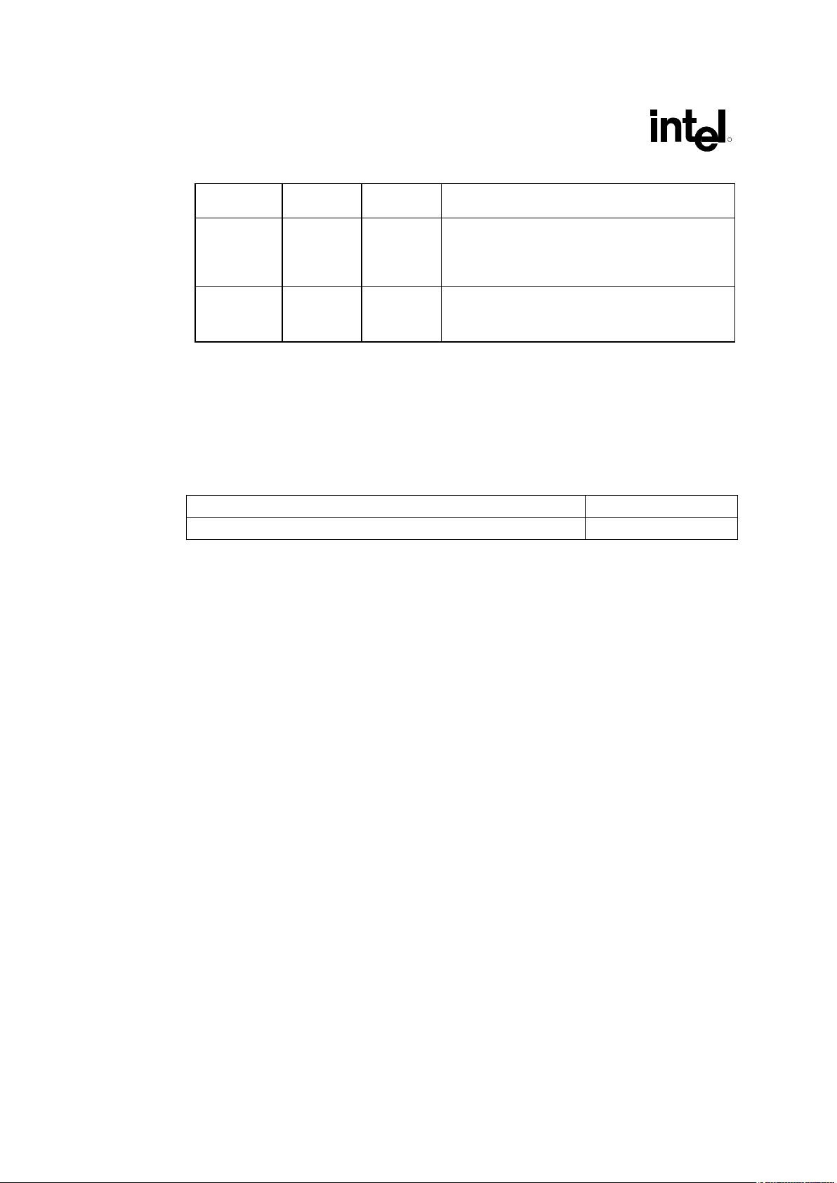
Signal Definition
R
10 251289-001
Signal Peripheral Host Description
LPCPD# I O Power Down: Indicates that the peripheral should
prepare for power to be removed from the LPC I/F
devices. Actual power removal is system dependent. This
signal is optional for the host.
LSMI# OD I SMI#: Only needed if peripheral want to cause SMI# on
an I/O instruction for retry. Otherwise can use SMI# via
SERIRQ. This signal is optional for the host.
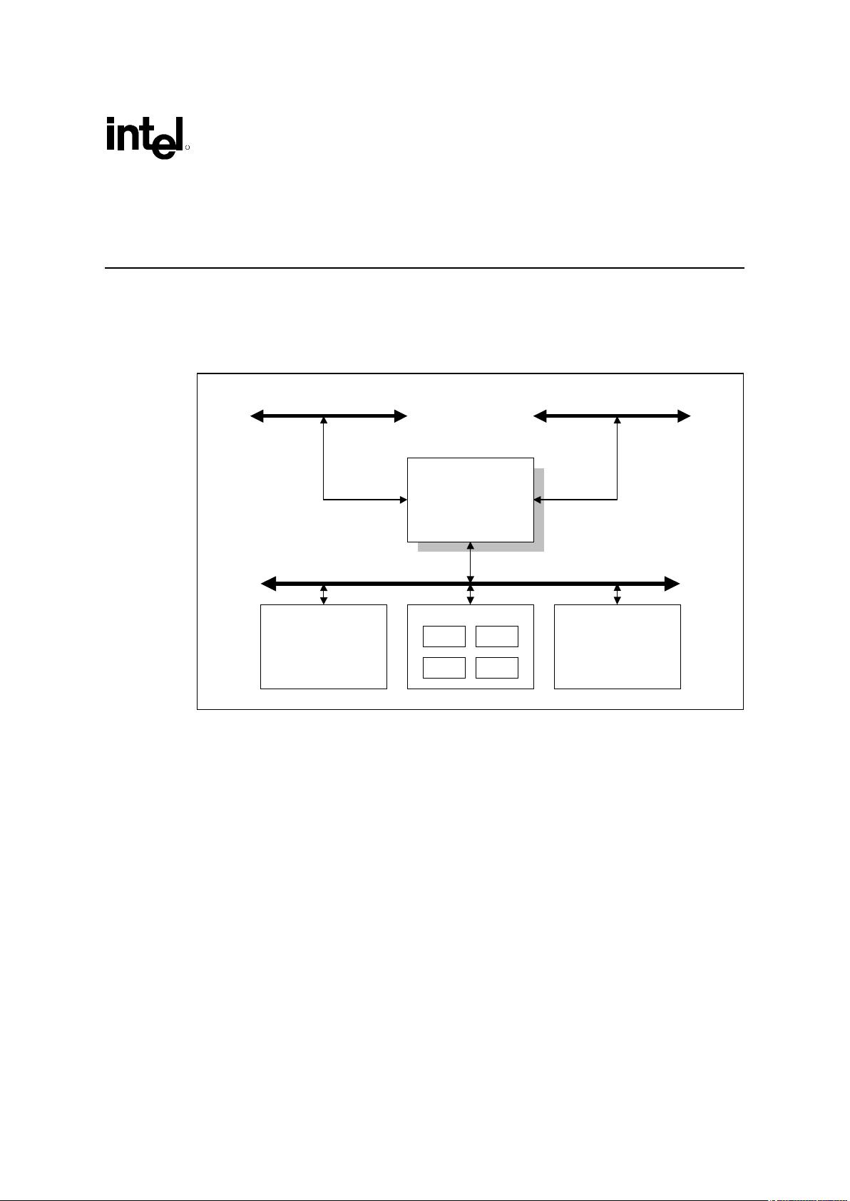
In comparison with existing ISA-based devices, the signal savings is substantial. The LPC
interface will generally only require 6 new signals: LAD[0:3], LFRAME#, and LDRQ#.
CLKRUN# is typically only implemented in mobile systems. LPCPD# is only needed for LPC
devices that are partially powered during certain low-power states.
At a minimum, the following ISA/X-bus signals found on plug-n-play devices are no longer
needed:
D[7:0], SA[15:0], DREQ[3:0], DACK#[3:0], TC, IOR#, IOW#, IOCHRDY 36 signals
Net Savings on Peripheral: 30
On 16 bit ISA based devices, the IOCS16# and MEMCS# signals are also saved. If the serial IRQ
was not previously supported, and if 16 bit DMA channels are used by the peripheral, several more
pins are saved. The net effect is that a fully functional Super I/O device that may have required a
160 pin package to implement can now fit in an 88 pin or less size package by using the LPC
interface.
剩余53页未读,继续阅读
相关推荐


cigarliang1
- 粉丝: 0
 我的内容管理
展开
我的内容管理
展开


最新资源
- Weblogic功能详解及使用手册
- 软件自动化测试资料分析与应用
- C++实现Joseph问题:nlgn时间算法与平衡二叉树
- VB字符判断程序:菜鸟的实践与交流
- 掌握Lucene全文索引:搜索实例演示
- Helloer_v1.8版发布:全面的技术文档与安装资源
- 掌握NS2网络仿真工具:步骤与分析
- Proteus仿真Max7221动态显示实用教程
- C#纸业销售管理系统开发与下载指南
- LWUIT J2ME界面设计实例与Eclipse项目转换
- MP3剪切软件工具:轻松编辑你的音乐文件
- JSP与SQL结合的人事管理系统开发教程
- 梁昆淼数学物理方法习题解答精编
- 批量将Word文档转换为Flash文档工具
- Pbkiller 2.5.8:Powerbuilder文件反编译神器
- USB开发基础教程与驱动结构分析
- 掌握CVS使用与安装:完整基础教程与软件下载
- 网页制作遇到的问题与解决方案集锦
- L7手机连接必备:高效USB驱动安装指南
- C#实现的人力资源管理系统代码分析
- MFC实现ODBC数据库闹钟功能
- Win32系统服务开发深度解析与实战案例
- Java+Swing开发的企业人事管理系统研究
- 计算机行业翻译利器:专业英语翻译软件
