没有合适的资源?快使用搜索试试~ 我知道了~
首页赛微CW2017 datasheet.pdf
资源详情
资源评论
资源推荐
www.cellwise-semi.com CW2017-DS V1.0
© 2018-2019 Cellwise Microelectronics 1
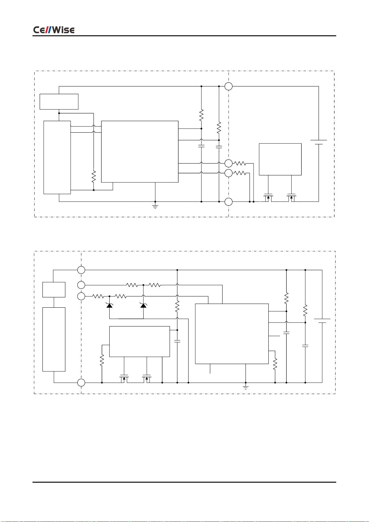
CW2017
Lithium-ion Fuel Gauge IC with ID Measurement Function
Features
System-Side or Pack-Side Fuel Gauging
±3% Maximum SOC Measurement Error
14-bit Sigma-Delta ADC for Cell Voltage,
Temperature and ID Resistor Measurement
Configurable Interrupt for Battery SOC Change,
High or Low Battery Temperature
No Offset Accumulation During Life Time
No Full-to-Empty Battery Learning Cycle
No Sense Resistor Required
Patented “FastCali” Fuel Gauging Algorithm
External Thermistor Supported
ID Resistor Measurement Supported
Ultra-low Power Consumption
Normal Mode 17A
Sleep Mode <1A
General I
2
C Interface
Tiny, Lead(Pb)-Free, TDFN 2mmx2mm-8L
Package
Applications
Smartphone
Tablet PCs
Handheld and Portable Devices
Lithium-ion or Lithium Polymer Battery Packs
General Description
The CW2017 is an ultra-compact, system-side or
pack-side, sensing resistor free, fuel gauging IC for
Lithium-ion(Li+) based batteries in handheld and
portable devices.
The CW2017 tracks the Li+ battery’s operation
conditions and performs state-of-the-art algorithm
to calculate the relative State-of-Charge (SOC) of
very different battery chemistry systems (LiCoOx,
polymer Li-ion, LiMnOx etc.).
The CW2017 includes a 14-bit Sigma-Delta ADC,
a precision voltage reference and build-in NTC
bias circuits. The IC allows users to eliminate the
expensive current sensing resistor which usually
occupies very large PCB area. The IC sends out
the alarm signal if the battery SOC level or the
temperature measured reaches the pre-
programmed threshold.
The CW2017 integrates the ID resistor sensing
feature. It can also be used as an alternative
sensing port.
The CW2017 uses a 2-wire I
2
C compatible serial
interface that operates in standard (100kHz) mode
or fast (400kHz) mode.
CW2017
2 © 2018-2019 Cellwise Microelectronics
Application Circuits
CW2017
Power
Supply
μP
Protection
IC
SCL
SDA
INT_N
VCC
VSS
VCELL
470
100
4.7K
1.0μF
1.0μF
System
Battery Pack
I2C
Master
INT
P+P+
P-
ID
NTC
VDD
ID
TS
Figure 1. Typical Application Diagram (System Side)
Figure1 is a typical application diagram of CW2017 used in system side, recommended external
components are marked on the figure.
CW2017
Power
Supply
μP
Protection
IC
SCL SDA
VCC
VSS
VCELL
VDD
ID
TS
470
100
1.0μF
1.0μF
System
Battery Pack
VM
VSS
VDD
I2C
P+
P-
100 100
100 100
4.7V 4.7V
INT_N
NTC
Figure 2. Typical Application Diagram (Pack Side)
Figure 2 is a typical application diagram of CW2017 used in pack side, recommended external components
are marked on the figure.
The CW2017 can be used in application with multi-battery connected in series or in parallel. Please refers
to the application note for more information or contacts support@cellwise-semi.com for more support.
CW2017
© 2018-2019 Cellwise Microelectronics 3
Ordering Information
PART
OPERATING
TEMPERATURE
PACKAGE
TOP MARK
CW2017AAAD
-40
o
C to 85
o
C
TDFN8
2017XXXX
Note: XXXX stands for the manufacture info.
Pin Configuration
TDFN Package Top view
2mm*2mm – 8pin
(Pad Side Down)
Pin Descriptions
PIN
NAME
DESCRIPTION
1
ID
ID measuring I/O. It can be left floating if unused.
2
VCELL
Battery voltage monitor I/O.
3
VDD
System power supply.
4
VSS
General purpose ground connection.
5
INT_N
Alarm signal for MCU interrupt controller. It can be left floating if unused.
6
TS
Thermistor measuring I/O.
7
SCL
Serial clock input.
8
SDA
Serial data input/output.
1 2 3 4
8 7 6 5
CW2017
CW2017
4 © 2018-2019 Cellwise Microelectronics
Type Number
CW2017XXXX
Package type D: TDFN 2mm*2mm-8L;
Parameter generation A: Standard firmware and parameter, A version
Standard Li+ battery application A: CellWise Li-Polymer profile
Function and revision A: A generation product
Absolute Maximum Ratings
VALUE
UNITS
MIN
MAX
Voltage respect to VSS
ID, CELL, VDD, INT_N, TS, SCL, SDA
-0.3
6
V
Output Current
INT_N, SDA
10
mA
Operation Temperature
T
A
-40
85
°C
Junction Temperature
T
J
-40
150
°C
Storage Temperature
T
STG
-50
150
°C
ESD
All pins. HBM model.
±2000
V
Moisture Sensitivity Level
MSL
Level 3
Caution:
Stresses beyond "Absolute Maximum Ratings" condition may cause permanent damage to the device.
These are stress ratings only and functional operation of the device at these or any other beyond those
indicated in the operational sections of the specifications is not implied. Exposure to absolute maximum
rating conditions for extended periods may affect device reliability.
Recommended DC Operating Conditions
PARAMETER
DESCRIPTION
MIN
MAX
UNITS
Input Voltage Range
ID, VCELL, VDD, INT_N, TS, SCL, SDA
-0.3
5.5
V
I
2
C Clock Frequency
400
kHz
Operation Temperature
-40
85
℃
剩余16页未读,继续阅读
xiaoxin726
- 粉丝: 1
- 资源: 11
上传资源 快速赚钱
- 我的内容管理 收起
- 我的资源 快来上传第一个资源
- 我的收益 登录查看自己的收益
- 我的积分 登录查看自己的积分
- 我的C币 登录后查看C币余额
- 我的收藏
- 我的下载
- 下载帮助
会员权益专享
最新资源
- zigbee-cluster-library-specification
- JSBSim Reference Manual
- c++校园超市商品信息管理系统课程设计说明书(含源代码) (2).pdf
- 建筑供配电系统相关课件.pptx
- 企业管理规章制度及管理模式.doc
- vb打开摄像头.doc
- 云计算-可信计算中认证协议改进方案.pdf
- [详细完整版]单片机编程4.ppt
- c语言常用算法.pdf
- c++经典程序代码大全.pdf
- 单片机数字时钟资料.doc
- 11项目管理前沿1.0.pptx
- 基于ssm的“魅力”繁峙宣传网站的设计与实现论文.doc
- 智慧交通综合解决方案.pptx
- 建筑防潮设计-PowerPointPresentati.pptx
- SPC统计过程控制程序.pptx
资源上传下载、课程学习等过程中有任何疑问或建议,欢迎提出宝贵意见哦~我们会及时处理!
点击此处反馈
安全验证
文档复制为VIP权益,开通VIP直接复制
信息提交成功
评论5