
1
Page 1
1
Ker’2K
ESD Protection Techniques
in Deep-Submicron CMOS Technology
Dr. Ming-Dou Ker
Integrated Circuits & Systems Laboratory
Institute of Electronics
National Chiao-Tung University, Hsinchu, Taiwan
mdker@ieee.org
Sept. 2000
2
Ker’2K
OUTLINE
1. Models of ESD Events.
2. ESD Specifications for IC Products.
3. Pin Combination in ESD Testing.
4. Design Concept of On-Chip ESD Protection.
5. Process Issues on ESD Robustness.
6. Recent Advances in CMOS On-Chip ESD Protection
Techniques.
7. Whole-Chip ESD Protection Scheme.
8. Conclusion and Discussion
3
3
Ker’2K
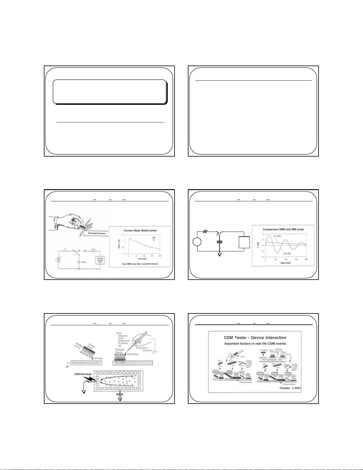
Models of ESD (Electrostatic Discharge) Events
(1). Human Body Model (HBM)
Standards :
1. MIL-STD-833C Method 3015.7
2. EIA/JESD22-A114-A (JEDEC, 1997)
3. ESD STM 5.1 (EOS/ESD, 1998)
CHBM= 100pF; RHBM= 1.5k
Ω
4
4
Ker’2K
Models of ESD (Electrostatic Discharge) Events
(2). Machine Model (MM)
Standards :
1. EIAJ-IC-121 Method 20
2. EIA/JESD22-A115-A (JEDEC, 1997)
3. ESD STM 5.2 (EOS/ESD, 1999)
CMM= 200pF
RMM= 0
Ω
VESD
Device
Under
TestC=200pF
GND
Rg
5
5
Ker’2K
Models of ESD (Electrostatic Discharge) Events
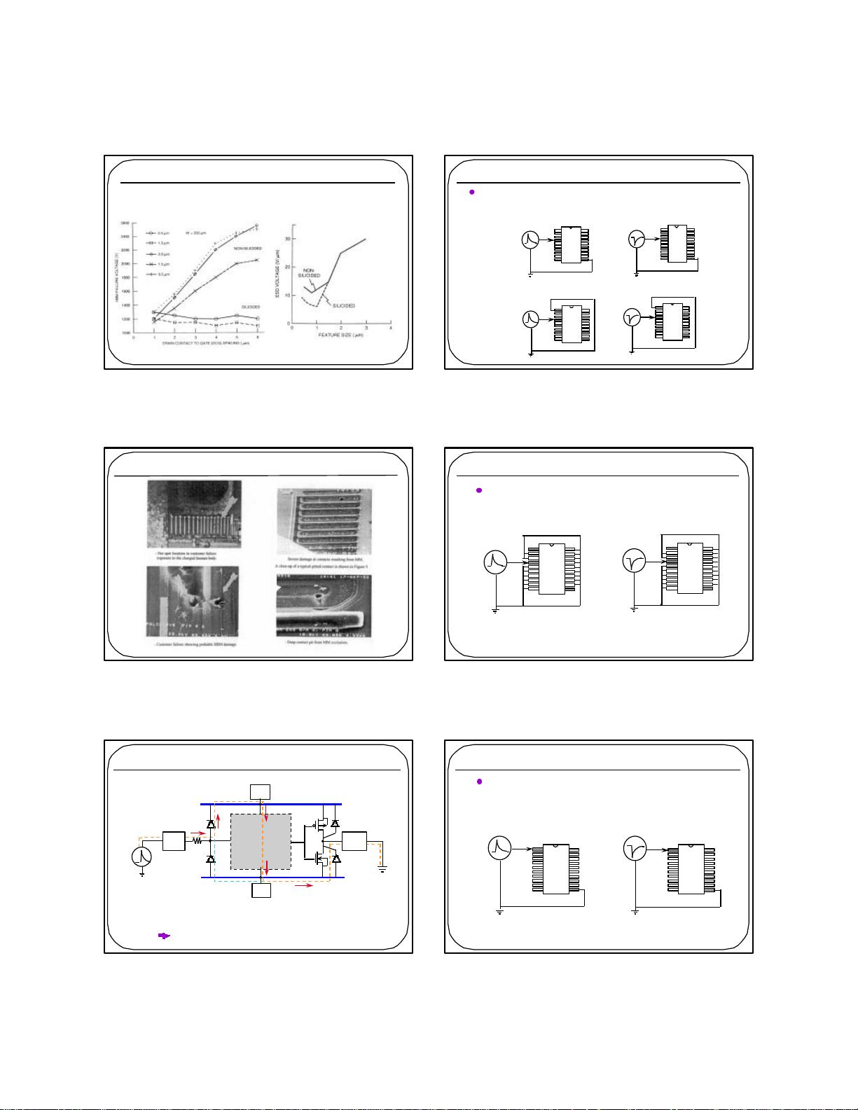
(3). Charged Device Model (CDM)
Standards :
1. JESD22-C101 (JEDEC, 1997)
2. ESD DS5.3.1 (EOS/ESD, 1996)
CCDM
6
6
Ker’2K
Models of ESD (Electrostatic Discharge) Events
(3). Charged Device Model (CDM)
Different dies and packages cause different ESD voltages in the CDM ESD events.
剩余14页未读,继续阅读

sunny1889
- 粉丝: 0
- 资源: 2
 我的内容管理
收起
我的内容管理
收起
- 我的资源
快来上传第一个资源
 我的收益 登录查看自己的收益
 我的积分
登录查看自己的积分
我的积分
登录查看自己的积分
 我的C币
登录后查看C币余额
我的C币
登录后查看C币余额
 我的收藏
我的收藏  我的下载
我的下载  下载帮助
下载帮助

会员权益专享


最新资源
- c++校园超市商品信息管理系统课程设计说明书(含源代码) (2).pdf
- 建筑供配电系统相关课件.pptx
- 企业管理规章制度及管理模式.doc
- vb打开摄像头.doc
- 云计算-可信计算中认证协议改进方案.pdf
- [详细完整版]单片机编程4.ppt
- c语言常用算法.pdf
- c++经典程序代码大全.pdf
- 单片机数字时钟资料.doc
- 11项目管理前沿1.0.pptx
- 基于ssm的“魅力”繁峙宣传网站的设计与实现论文.doc
- 智慧交通综合解决方案.pptx
- 建筑防潮设计-PowerPointPresentati.pptx
- SPC统计过程控制程序.pptx
- SPC统计方法基础知识.pptx
- MW全能培训汽轮机调节保安系统PPT教学课件.pptx
资源上传下载、课程学习等过程中有任何疑问或建议,欢迎提出宝贵意见哦~我们会及时处理!
点击此处反馈


评论1