没有合适的资源?快使用搜索试试~ 我知道了~
首页电流输出dac7612
电流输出dac7612
5星 · 超过95%的资源 需积分: 46 19 下载量 47 浏览量
更新于2023-03-03
评论
收藏 126KB PDF 举报
一个电流输出模块资料 一个电流输出模块资料 一个电流输出模块资料 一个电流输出模块资料
资源详情
资源评论
资源推荐
© 1999 Burr-Brown Corporation PDS-1501A Printed in U.S.A. June, 1999
International Airport Industrial Park • Mailing Address: PO Box 11400, Tucson, AZ 85734 • Street Address: 6730 S. Tucson Blvd., Tucson, AZ 85706 • Tel: (520) 746-1111
Twx: 910-952-1111 • Internet: http://www.burr-brown.com/ • Cable: BBRCORP • Telex: 066-6491 • FAX: (520) 889-1510 • Immediate Product Info: (800) 548-6132
®
DAC7612
Dual, 12-Bit Serial Input
DIGITAL-TO-ANALOG CONVERTER
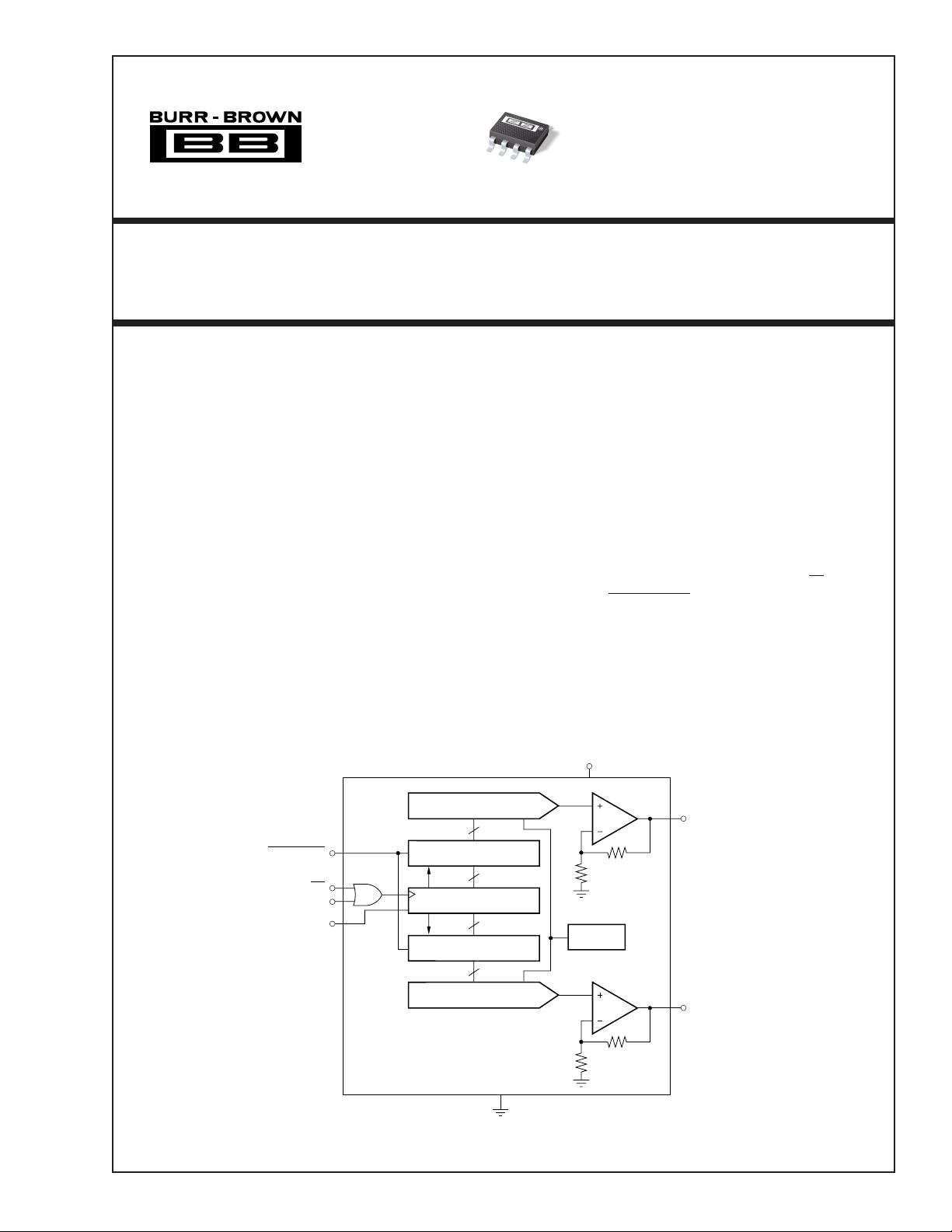
DESCRIPTION
The DAC7612 is a dual, 12-bit digital-to-analog con-
verter (DAC) with guaranteed 12-bit monotonicity
performance over the industrial temperature range. It
requires a single +5V supply and contains an input
shift register, latch, 2.435V reference, a dual DAC, and
high speed rail-to-rail output amplifiers. For a full-
scale step, each output will settle to 1 LSB within 7µs
while only consuming 3.7mW.
The synchronous serial interface is compatible with a
wide variety of DSPs and microcontrollers. Clock
(CLK), Serial Data In (SDI), Chip Select (CS) and
Load DACs (LOADDACS) comprise the serial inter-
face.
The DAC7612 is available in an 8-lead SOIC package
and is fully specified over the industrial temperature
range of –40°C to +85°C.
FEATURES
● LOW POWER: 3.7mW
● FAST SETTLING: 7µs to 1 LSB
● 1mV LSB WITH 4.095V FULL-SCALE
RANGE
● COMPLETE WITH REFERENCE
● 12-BIT LINEARITY AND MONOTONICITY
OVER INDUSTRIAL TEMP RANGE
● 3-WIRE INTERFACE: Up to 20MHz Clock
● SMALL PACKAGE: 8-Lead SOIC
APPLICATIONS
● PROCESS CONTROL
● DATA ACQUISITION SYSTEMS
● CLOSED-LOOP SERVO-CONTROL
● PC PERIPHERALS
● PORTABLE INSTRUMENTATION
DAC7612
12-Bit DAC A
DAC Register A
14-Bit Serial Shift Register
12
12
DAC Register B
Ref
12
12
LOADDACS
CS
CLK
SDI
V
DD
GND
V
OUTA
DAC7612
12-Bit DAC B
V
OUTB
SBAS106
2
®
DAC7612
SPECIFICATIONS
At T
A
= –40°C to +85°C, and V
DD
= +5V, unless otherwise noted.
The information provided herein is believed to be reliable; however, BURR-BROWN assumes no responsibility for inaccuracies or omissions. BURR-BROWN assumes
no responsibility for the use of this information, and all use of such information shall be entirely at the user’s own risk. Prices and specifications are subject to change
without notice. No patent rights or licenses to any of the circuits described herein are implied or granted to any third party. BURR-BROWN does not authorize or warrant
any BURR-BROWN product for use in life support devices and/or systems.
DAC7612U DAC7612UB
PARAMETER CONDITIONS MIN TYP MAX MIN TYP MAX UNITS
RESOLUTION 12 ✻ Bits
ACCURACY
Relative Accuracy
(1)
–2 ±1/2 +2 –1 ±1/4 +1 LSB
Differential Nonlinearity Guaranteed Monotonic –1 ±1/2 +1 –1 ±1/4 +1 LSB
Zero-Scale Error Code 000
H
–1 +1 +3 ✻✻✻ LSB
Zero Scale Match Code 000
H
1/2 1/2 2 LSB
Full-Scale Voltage Code FFF
H
4.079 4.095 4.111 4.087 4.095 4.103 V
Full-Scale Match Code FFF
H
1/2 1/2 2 LSB
ANALOG OUTPUT
Output Current Code 800
H
±5 ±7 ✻✻ mA
Load Regulation R
LOAD
≥ 402Ω, Code 800
H
13 ✻✻ LSB
Capacitive Load No Oscillation 500 ✻ pF
Short-Circuit Current ±15 ✻ mA
Short-Circuit Duration GND or V
DD
Indefinite ✻
DIGITAL INPUT
Data Format Serial ✻
Data Coding Straight Binary ✻
Logic Family CMOS ✻
Logic Levels
V
IH
0.7 • V
DD
✻ V
V
IL
0.3 • V
DD
✻ V
I
IH
±10 ✻ µA
I
IL
±10 ✻ µA
DYNAMIC PERFORMANCE
Settling Time
(2)
(t
S
) To ±1 LSB of Final Value 7 ✻ µs
DAC Glitch 2.5 ✻ nV-s
Digital Feedthrough 0.5 ✻ nV-s
POWER SUPPLY
V
DD
+4.75 +5.0 +5.25 ✻✻✻ V
I
DD
V
IH
= 5V, V
IL
= 0V, No Load, at Code 000
H
0.75 1.5 ✻✻ mA
Power Dissipation V
IH
= 5V, V
IL
= 0V, No Load 3.5 7.5 ✻✻ mW
Power Supply Sensitivity ∆V
DD
= ±5% 0.0025 0.002 ✻✻%/%
TEMPERATURE RANGE
Specified Performance –40 +85 ✻✻°C
✻ Same specification as for DAC7612U.
NOTES: (1) This term is sometimes referred to as Linearity Error or Integral Nonlinearity (INL). (2) Specification does not apply to negative-going transitions where
the final output voltage will be within 3 LSBs of ground. In this region, settling time may be double the value indicated.
3
®
DAC7612
PIN CONFIGURATION
Top View SO-8
V
DD
to GND .......................................................................... –0.3V to 6V
Digital Inputs to GND ..............................................–0.3V to V
DD
+ 0.3V
V
OUT
to GND ...........................................................–0.3V to V
DD
+ 0.3V
Power Dissipation ........................................................................ 325mW
Thermal Resistance,
θ
JA
........................................................... 150°C/W
Maximum Junction Temperature ..................................................+150°C
Operating Temperature Range ...................................... –40°C to +85°C
Storage Temperature Range ....................................... –65°C to +150°C
Lead Temperature (soldering, 10s) .............................................. +300°C
NOTE: (1) Stresses above those listed under “Absolute Maximum Ratings”
may cause permanent damage to the device. Exposure to absolute maximum
conditions for extended periods may affect device reliability.
ABSOLUTE MAXIMUM RATINGS
(1)
PIN DESCRIPTIONS
PIN LABEL DESCRIPTION
1 SDI Serial Data Input. Data is clocked into the internal
serial register on the rising edge of CLK.
2 CLK Synchronous Clock for the Serial Data Input.
3 LOADDACS Loads the internal DAC registers. All DAC registers
are transparent latches and are transparent when
LOADDACS is LOW (regardless of the state of CS
or CLK).
4 CS Chip Select. Active LOW.
5V
OUTB
DAC B Output Voltage
6 GND Ground
7V
DD
Positive Power Supply
8V
OUTA
DAC A Output Voltage
ELECTROSTATIC
DISCHARGE SENSITIVITY
This integrated circuit can be damaged by ESD. Burr-Brown
recommends that all integrated circuits be handled with
appropriate precautions. Failure to observe proper handling
and installation procedures can cause damage.
ESD damage can range from subtle performance degrada-
tion to complete device failure. Precision integrated circuits
may be more susceptible to damage because very small
parametric changes could cause the device not to meet its
published specifications.
PACKAGE/ORDERING INFORMATION
MINIMUM
RELATIVE DIFFERENTIAL SPECIFICATION PACKAGE
ACCURACY NONLINEARITY TEMPERATURE DRAWING ORDERING TRANSPORT
PRODUCT (LSB) (LSB) RANGE PACKAGE NUMBER
(1)
NUMBER
(2)
MEDIA
DAC7612U ±2 ±1 –40°C to +85°C SO-8 182 DAC7612U Rails
"" " " ""DAC7612U/2K5 Tape and Reel
DAC7612UB ±1 ±1 –40°C to +85°C SO-8 182 DAC7612UB Rails
"" " " ""DAC7612UB/2K5 Tape and Reel
NOTES: (1) For detailed drawing and dimension table, please see end of data sheet, or Appendix C of Burr-Brown IC Data Book. (2) Models with a slash (/) are
available only in Tape and Reel in the quantities indicated (e.g., /2K5 indicates 2500 devices per reel). Ordering 2500 pieces of “DAC7612U/2K5” will get a single
2500-piece Tape and Reel. For detailed Tape and Reel mechanical information, refer to Appendix B of Burr-Brown IC Data Book.
1
2
3
4
8
7
6
5
SDI
CLK
LOADDACS
CS
V
OUTA
V
DD
GND
V
OUTB
DAC7612U
剩余12页未读,继续阅读
yyc710903
- 粉丝: 0
- 资源: 12
上传资源 快速赚钱
- 我的内容管理 收起
- 我的资源 快来上传第一个资源
- 我的收益 登录查看自己的收益
- 我的积分 登录查看自己的积分
- 我的C币 登录后查看C币余额
- 我的收藏
- 我的下载
- 下载帮助
会员权益专享
最新资源
- 27页智慧街道信息化建设综合解决方案.pptx
- 计算机二级Ms-Office选择题汇总.doc
- 单链表的插入和删除实验报告 (2).docx
- 单链表的插入和删除实验报告.pdf
- 物联网智能终端项目设备管理方案.pdf
- 如何打造品牌的模式.doc
- 样式控制与页面布局.pdf
- 武汉理工Java实验报告(二).docx
- 2021线上新品消费趋势报告.pdf
- 第3章 Matlab中的矩阵及其运算.docx
- 基于Web的人力资源管理系统的必要性和可行性.doc
- 基于一阶倒立摆的matlab仿真实验.doc
- 速运公司物流管理模式研究教材
- 大数据与管理.pptx
- 单片机课程设计之步进电机.doc
- 大数据与数据挖掘.pptx
资源上传下载、课程学习等过程中有任何疑问或建议,欢迎提出宝贵意见哦~我们会及时处理!
点击此处反馈
安全验证
文档复制为VIP权益,开通VIP直接复制
信息提交成功
评论1