
© 2007 OmniVision Technologies, Inc. VarioPixel, OmniVision, and the OmniVision logo are registered trademarks of OmniVision Technologies, Inc.
Version 1.4, December 17, 2007 OmniPixel2 and CameraChip are trademarks of OmniVision Technologies, Inc.
These specifications are subject to change without notice.
Advanced Information
Datasheet
OV7725 Color CMOS VGA (640x480) CAMERACHIP
TM
Sensor
O
mni ision
®
with OmniPixel2
TM
Technology
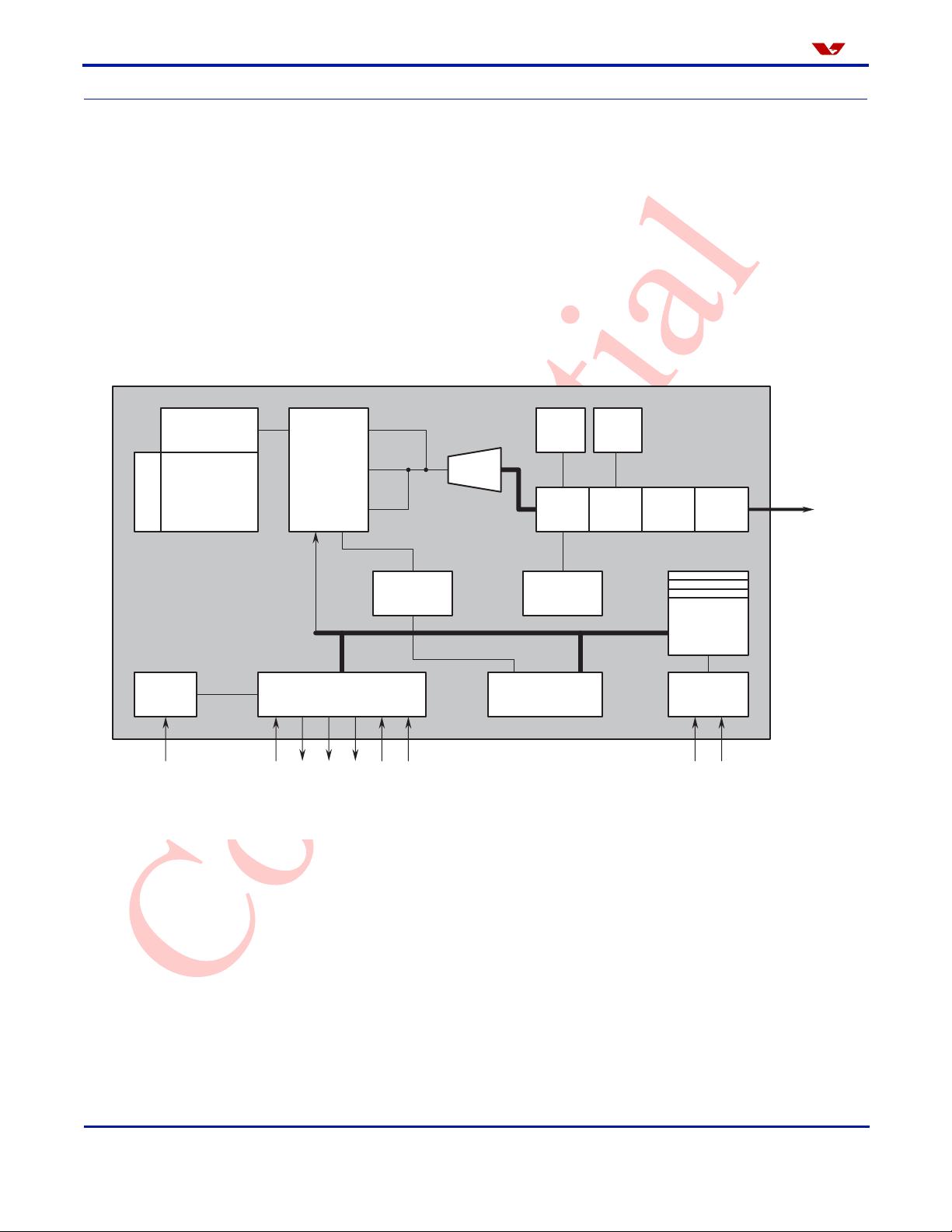
General Description
The OV7725 CAMERACHIP™ image sensor is a low
voltage CMOS device that provides the full functionality of
a single-chip VGA camera and image processor in a small
footprint package. The OV7725 provides full-frame,
sub-sampled or windowed 8-bit/10-bit images in a wide
range of formats, controlled through the Serial Camera
Control Bus (SCCB) interface.
This device has an image array capable of operating at up
to 60 frames per second (fps) in VGA with complete user
control over image quality, formatting and output data
transfer. All required image processing functions,
including exposure control, gamma, white balance, color
saturation, hue control and more, are also programmable
through the SCCB interface. In addition, OmniVision
sensors use proprietary sensor technology to improve
image quality by reducing or eliminating common
lighting/electrical sources of image contamination, such
as fixed pattern noise, smearing, blooming, etc., to
produce a clean, fully stable color image.
Features
• High sensitivity for low-light operation
• Standard SCCB interface
• Output support for Raw RGB, RGB (GRB 4:2:2,
RGB565/555/444) and YCbCr (4:2:2) formats
• Supports image sizes: VGA, QVGA, and any size
scaling down from CIF to 40x30
• VarioPixel
®
method for sub-sampling
• Automatic image control functions including:
Automatic Exposure Control (AEC), Automatic Gain
Control (AGC), Automatic White Balance (AWB),
Automatic Band Filter (ABF), and Automatic
Black-Level Calibration (ABLC)
• Image quality controls including color saturation,
hue, gamma, sharpness (edge enhancement), and
anti-blooming
• ISP includes noise reduction and defect correction
• Lens shading correction
• Saturation level auto adjust (UV adjust)
• Edge enhancement level auto adjust
• De-noise level auto adjust
• Frame synchronization capability
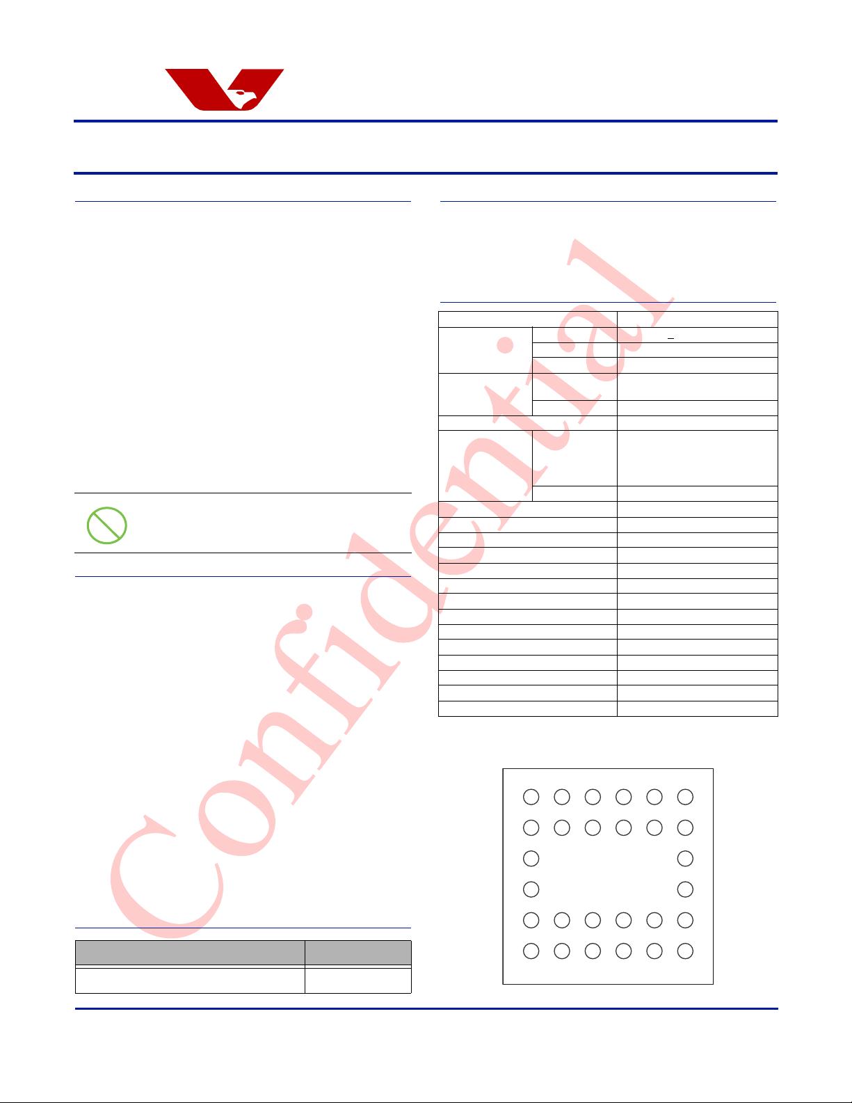
Ordering Information
Pb
Note: The OV7725 uses a lead-free
package.
Product Package
OV07725-VL1A (Color, lead-free) 28-pin CSP2
Applications
• Cellular and picture phones
•Toys
• PC Multimedia
• Digital still cameras
Key Specifications
Figure 1 OV7725 Pinout (Top View)
Array Size 640 x 480
Power Supply
Digital Core 1.8VDC +
10%
Analog 3.0V to 3.6V
I/O 1.7V to 3.3V
Power
Requirements
Active
120 mW typical
(60 fps VGA, YUV)
Standby < 20 µA
Temperature Range -20°C to +70°C
Output Format
8-bit
• YUV/YCbCr 4:2:2
• RGB565/555/444
• GRB 4:2:2
•Raw RGB Data
10-bit
•Raw RGB Data
Lens Size 1/4"
Lens Chief Ray Angle 25° non linear
Max Image Transfer Rate 60 fps for VGA
Sensitivity 3.8 V/(Lux
• sec)
S/N Ratio 50 dB
Dynamic Range 60 dB
Scan Mode Progressive
Electronic Exposure Up to 510:1 (for selected fps)
Pixel Size 6.0 µm x 6.0 µm
Dark Current 40 mV/s
Well Capacity 26 Ke
-
Fixed Pattern Noise < 0.03% of V
PEAK-TO-PEAK
Image Area 3984 µm x 2952 µm
Package Dimensions 5345 µm x 5265 µm
A1
ADVDD
A2
RSTB
A3
VREFH
OV7725
A4
FSIN
A5
SCL
B1
ADGND
B2
VREFN
B4
AGND
B3
AVDD
B5
SDA
C1
PWDN
D1
D5
E1
D7
E2
D1
E5
DOVDD
F1
D9
F2
D3
F3
XCLK
F4
DOGND
F5
D2
A6
D0
B6
HREF
C6
VSYNC
D6
D4
E6
D6
F6
D8
E3
DVDD
E4
PCLK
7725CSP_DS_001


剩余43页未读,继续阅读

rickliu74
- 粉丝: 0
- 资源: 8
 我的内容管理
收起
我的内容管理
收起
- 我的资源
快来上传第一个资源
 我的收益 登录查看自己的收益
 我的积分
登录查看自己的积分
我的积分
登录查看自己的积分
 我的C币
登录后查看C币余额
我的C币
登录后查看C币余额
 我的收藏
我的收藏  我的下载
我的下载  下载帮助
下载帮助

会员权益专享


最新资源
- c++校园超市商品信息管理系统课程设计说明书(含源代码) (2).pdf
- 建筑供配电系统相关课件.pptx
- 企业管理规章制度及管理模式.doc
- vb打开摄像头.doc
- 云计算-可信计算中认证协议改进方案.pdf
- [详细完整版]单片机编程4.ppt
- c语言常用算法.pdf
- c++经典程序代码大全.pdf
- 单片机数字时钟资料.doc
- 11项目管理前沿1.0.pptx
- 基于ssm的“魅力”繁峙宣传网站的设计与实现论文.doc
- 智慧交通综合解决方案.pptx
- 建筑防潮设计-PowerPointPresentati.pptx
- SPC统计过程控制程序.pptx
- SPC统计方法基础知识.pptx
- MW全能培训汽轮机调节保安系统PPT教学课件.pptx
资源上传下载、课程学习等过程中有任何疑问或建议,欢迎提出宝贵意见哦~我们会及时处理!
点击此处反馈


评论8