没有合适的资源?快使用搜索试试~ 我知道了~
首页16位高速数模转换芯片AD7705资料
16位高速数模转换芯片AD7705资料
需积分: 50 34 下载量 144 浏览量
更新于2023-03-03
评论 1
收藏 264KB PDF 举报
AD7705/06芯片是带有自校正功能的Σ-Δ于A/D转换器。其内部由多路模拟 开关、缓冲器、可编程增益放大器(PGA)、Σ-Δ调制器、数字滤波器、基准电压输入、时钟电路及串行接口组成。其中串行接口包括寄存器组,它由通讯寄存器、设置寄存器、时钟寄存器、数据输出寄存器、零点校正寄存器和满程校正寄存器等组成。该芯片还包括2通道差分输入(AD7705)和3种伪差分通道输入(AD7706)。 AD7705/06的PGA可通过指令设定,对不同幅度的输入信号实现1、2、4、8、16、32、64和128倍的放大,因此AD7705/06芯片既可接受从传感器送来的低电平输入信号,亦可接受高电平(10V)信号,它运用Σ―Δ技术实现16位无误码性能;它的输出速度同样可由指令设定,范围由 20Hz到500Hz;它能够通过指令设定对零点和满程进行校正;AD7705/06与微处理器的数据传送通过串行方式进行,采用了节省端口线的通讯方式,最少只占用控制机的两条端口线。
资源详情
资源评论
资源推荐
REV. A
Information furnished by Analog Devices is believed to be accurate and
reliable. However, no responsibility is assumed by Analog Devices for its
use, nor for any infringements of patents or other rights of third parties
which may result from its use. No license is granted by implication or
otherwise under any patent or patent rights of Analog Devices.
a
AD7705/AD7706
One Technology Way, P.O. Box 9106, Norwood, MA 02062-9106, U.S.A.
Tel: 781/329-4700 World Wide Web Site: http://www.analog.com
Fax: 781/326-8703 © Analog Devices, Inc., 1998
3 V/5 V, 1 mW
2-/3-Channel 16-Bit, Sigma-Delta ADCs
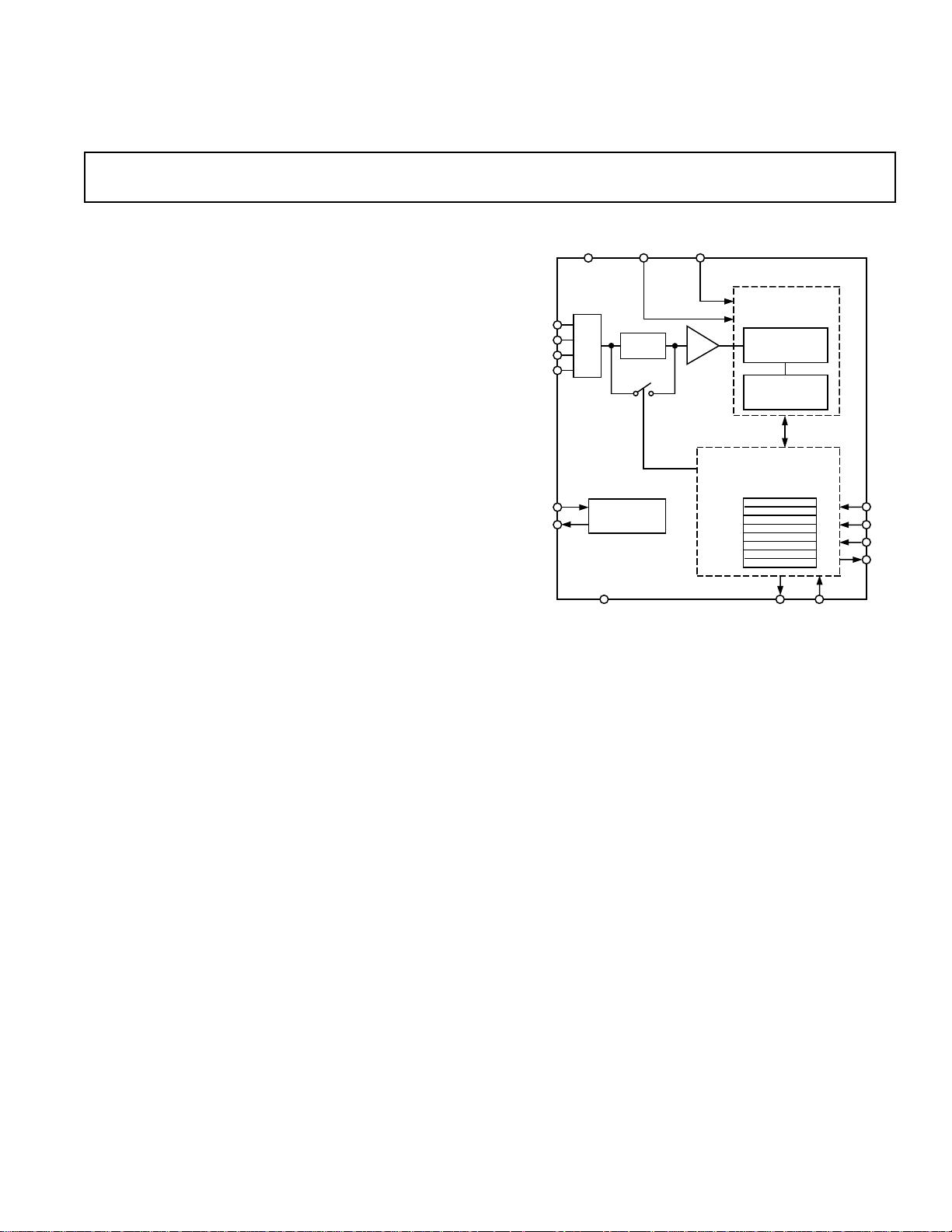
FUNCTIONAL BLOCK DIAGRAM
FEATURES
AD7705: Two Fully Differential Input Channel ADCs
AD7706: Three Pseudo Differential Input Channel ADCs
16 Bits No Missing Codes
0.003% Nonlinearity
Programmable Gain Front End
Gains from 1 to 128
Three-Wire Serial Interface
SPI™, QSPI™, MICROWIRE™ and DSP Compatible
Schmitt Trigger Input on SCLK
Ability to Buffer the Analog Input
2.7 V to 3.3 V or 4.75 V to 5.25 V Operation
Power Dissipation 1 mW max @ 3␣ V
Standby Current 8 A max
16-Lead DIP, 16-Lead SOIC and TSSOP Packages
GENERAL DESCRIPTION
The AD7705/AD7706 are complete analog front ends for low
frequency measurement applications. These two-/three-channel
devices can accept low level input signals directly from a trans-
ducer and produce a serial digital output. They employ a sigma-
delta conversion technique to realize up to 16 bits of no missing
codes performance. The selected input signal is applied to a
proprietary programmable gain front end based around an ana-
log modulator. The modulator output is processed by an on-
chip digital filter. The first notch of this digital filter can be
programmed via an on-chip control register allowing adjustment
of the filter cutoff and output update rate.
The AD7705/AD7706 operate from a single 2.7 V to 3.3 V or
4.75 V to 5.25 V supply. The AD7705 features two fully differ-
ential analog input channels while the AD7706 features three
pseudo differential input channels. Both devices feature a differ-
ential reference input. Input signal ranges of 0 mV to +20␣ mV
through 0 V to +2.5␣ V can be incorporated on both devices when
operating with a V
DD
of 5 V and a reference of 2.5 V. They can
also handle bipolar input signal ranges of ±20␣ mV through ±2.5␣ V,
which are referenced to the AIN(–) inputs on the AD7705 and to
the COMMON input on the AD7706. The AD7705/AD7706,
with 3 V supply and a 1.225 V reference, can handle unipolar
input signal ranges of 0 mV to +10␣ mV through 0 V to +1.225␣ V.
Its bipolar input signal ranges are ±10␣ mV through ±1.225␣ V.
The AD7705/AD7706 thus perform all signal conditioning and
conversion for a two- or three-channel system.
The AD7705/AD7706 are ideal for use in smart, microcontroller
or DSP-based systems. They feature a serial interface that can
be configured for three-wire operation. Gain settings, signal
polarity and update rate selection can be configured in software
using the input serial port. The part contains self-calibration and
system calibration options to eliminate gain and offset errors on
the part itself or in the system.
CMOS construction ensures very low power dissipation, and the
power-down mode reduces the standby power consumption to
20␣ µW typ. These parts are available in a 16-lead, 0.3 inch-wide,
plastic dual-in-line package (DIP), a 16-lead wide body (0.3
inch) small outline (SOIC) package and also a low profile 16-
lead TSSOP.
PRODUCT HIGHLIGHTS
1. The AD7705/AD7706 consumes less than 1 mW at 3 V
supplies and 1␣ MHz master clock, making it ideal for use in
low power systems. Standby current is less than 8␣ µA.
2. The programmable gain input allows the AD7705/AD7706
to accept input signals directly from a strain gage or trans-
ducer, removing a considerable amount of signal conditioning.
3. The AD7705/AD7706 is ideal for microcontroller or DSP
processor applications with a three-wire serial interface re-
ducing the number of interconnect lines and reducing the
number of opto-couplers required in isolated systems.
4. The part features excellent static performance specifications
with 16 bits, no missing codes, ±0.003% accuracy and low
rms noise (<600␣ nV). Endpoint errors and the effects of
temperature drift are eliminated by on-chip calibration op-
tions, which remove zero-scale and full-scale errors.
*
*Protected by U.S. Patent Number 5,134,401.
SPI and QSPI are trademarks of Motorola, Inc.
MICROWIRE is a trademark of National Semiconductor.
V
DD REF IN(–) REF IN(+)
AD7705/AD7706
MAX
PGA
BUFFER
CHARGE
BALANCING
A/D CONVERTER
S - D
MODULATOR
DIGITAL FILTER
A = 1<128
SERIAL INTERFACE
REGISTER BANK
CLOCK
GENERATION
MCLK IN
MCLK OUT
GND
DRDY RESET
DIN
DOUT
CS
SCLK
ANALOG
INPUT
CHANNELS
–2–
REV. A
AD7705/AD7706–SPECIFICATIONS
(V
DD
= +3 V or 5 V, REF IN(+) = +1.225␣ V with V
DD
= 3 V and +2.5 V
with V
DD
= 5 V; REF␣ IN(–) = GND; MCLK IN = 2.4576␣ MHz unless otherwise noted. All specifications T
MIN
to T
MAX
unless otherwise noted.)
Parameter B Version
1
Units Conditions/Comments
STATIC PERFORMANCE
No Missing Codes 16 Bits min Guaranteed by Design. Filter Notch < 60␣ Hz
Output Noise See Tables I and III Depends on Filter Cutoffs and Selected Gain
Integral Nonlinearity
2
±0.003 % of FSR max Filter Notch < 60␣ Hz. Typically ±0.0003%
Unipolar Offset Error See Note 3
Unipolar Offset Drift
4
0.5 µV/°C typ
Bipolar Zero Error See Note 3
Bipolar Zero Drift
4
0.5 µV/°C typ For Gains 1, 2 and 4
0.1 µV/°C typ For Gains 8, 16, 32, 64 and 128
Positive Full-Scale Error
5
See Note 3
Full-Scale Drift
4, 6
0.5 µV/°C typ
Gain Error
7
See Note 3
Gain Drift
4, 8
0.5 ppm of FSR/°C typ
Bipolar Negative Full-Scale Error
2
±0.003 % of FSR typ Typically ±0.001%
Bipolar Negative Full-Scale Drift
4
1 µV/°C typ For Gains of 1 to 4
0.6 µV/°C typ For Gains of 8 to 128
ANALOG INPUTS/REFERENCE INPUTS Specifications for AIN and REF IN Unless Noted
Input Common-Mode Rejection (CMR)
2
V
DD
= 5 V
Gain = 1 96 dB typ
Gain = 2 105 dB typ
Gain = 4 110 dB typ
Gain = 8v128 130 dB typ
V
DD
= 3 V
Gain = 1 105 dB typ
Gain = 2 110 dB typ
Gain = 4 120 dB typ
Gain = 8v128 130 dB typ
Normal-Mode 50 Hz Rejection
2
98 dB typ For Filter Notches of 25 Hz, 50 Hz, ±0.02 × f
NOTCH
Normal-Mode 60 Hz Rejection
2
98 dB typ For Filter Notches of 20 Hz, 60 Hz, ±0.02 × f
NOTCH
Common-Mode 50 Hz Rejection
2
150 dB typ For Filter Notches of 25 Hz, 50 Hz, ±0.02 × f
NOTCH
Common-Mode 60 Hz Rejection
2
150 dB typ For Filter Notches of 20 Hz, 60 Hz, ±0.02 × f
NOTCH
Absolute/Common-Mode REF IN Voltage
2
GND to V
DD
V min to V max
Absolute/Common-Mode AIN Voltage
2, 9
GND – 30 mV V min BUF Bit of Setup Register = 0
V
DD
+ 30␣ mV V max
Absolute/Common-Mode AIN Voltage
2, 9
GND + 50␣ mV V min BUF Bit of Setup Register = 1
V
DD
– 1.5␣ V V max
AIN DC Input Current
2
1 nA max
AIN Sampling Capacitance
2
10 pF max
AIN Differential Voltage Range
10
0 to +V
REF
/GAIN
11
nom Unipolar Input Range (B/U Bit of Setup Register = 1)
±V
REF
/GAIN nom Bipolar Input Range (B/U Bit of Setup Register = 0)
AIN Input Sampling Rate, f
S
GAIN × f
CLKIN
/64 For Gains of 1 to 4
f
CLKIN
/8 For Gains of 8 to 128
Reference Input Range
REF IN(+) – REF IN(–) Voltage 1/1.75 V min/max V
DD
= 2.7 V to 3.3 V. V
REF
= 1.225 ± 1% for Specified
Performance
REF IN(+) – REF IN(–) Voltage 1/3.5 V min/max V
DD
= 4.75 V to 5.25 V. V
REF
= 2.5 ± 1% for Specified
Performance
REF IN Input Sampling Rate, f
S
f
CLKIN
/64
LOGIC INPUTS
Input Current
All Inputs Except MCLK IN ±1 µA max Typically ±20 nA
MCLK ±10 µA max Typically ±2 µA
All Inputs Except SCLK and MCLK IN
V
INL
, Input Low Voltage 0.8 V max V
DD
= 5 V
0.4 V max V
DD
= 3 V
V
INH
, Input High Voltage 2.0 V min V
DD
= 3 V and 5 V
SCLK Only (Schmitt Triggered Input) V
DD
= 5 V NOMINAL
V
T+
1.4/3 V min/V max
V
T–
0.8/1.4 V min/V max
V
T+
– V
T–
0.4/0.8 V min/V max
SCLK Only (Schmitt Triggered Input) V
DD
= 3 V NOMINAL
V
T+
1/2.5 V min/V max
V
T–
0.4/1.1 V min/V max
V
T+
– V
T–
0.375/0.8 V min/V max
MCLK IN Only V
DD
= 5 V NOMINAL
V
INL
, Input Low Voltage 0.8 V max
V
INH
, Input High Voltage 3.5 V min
MCLK IN Only V
DD
= 3 V NOMINAL
V
INL
, Input Low Voltage 0.4 V max
V
INH
, Input High Voltage 2.5 V min
–3–REV. A
AD7705/AD7706
Parameter B Version
1
Units Conditions/Comments
LOGIC OUTPUTS (Including MCLK OUT)
V
OL
, Output Low Voltage 0.4 V max I
SINK
= 800␣ µA Except for MCLK OUT.
12
V
DD
= 5 V.
V
OL
, Output Low Voltage 0.4 V max I
SINK
= 100␣ µA Except for MCLK OUT.
12
V
DD
= 3 V.
V
OH
, Output High Voltage 4 V min I
SOURCE
= 200 µA Except for MCLK OUT.
12
V
DD
= 5 V.
V
OH
, Output High Voltage V
DD
–0.6 V min I
SOURCE
= 100␣ µA Except for MCLK OUT.
12
V
DD
= 3 V.
Floating State Leakage Current ±10 µA max
Floating State Output Capacitance
13
9 pF typ
Data Output Coding Binary Unipolar Mode
Offset Binary Bipolar Mode
SYSTEM CALIBRATION
Positive Full-Scale Calibration Limit
14
(1.05 × V
REF
)/GAIN V max GAIN Is the Selected PGA Gain (1 to 128)
Negative Full-Scale Calibration Limit
14
–(1.05 × V
REF
)/GAIN V max GAIN Is the Selected PGA Gain (1 to 128)
Offset Calibration Limit
14
–(1.05 × V
REF
)/GAIN V max GAIN Is the Selected PGA Gain (1 to 128)
Input Span
15
(0.8 × V
REF
)/GAIN V min GAIN Is the Selected PGA Gain (1 to 128)
(2.1 × V
REF
)/GAIN V max GAIN Is the Selected PGA Gain (1 to 128)
POWER REQUIREMENTS
V
DD
Voltage +2.7 to +3.3 V min to V max For Specified Performance
Power Supply Currents
16
Digital I/Ps = 0␣ V or V
DD
. External MCLK IN and
CLK DIS = 1
0.32 mA max BUF Bit = 0. f
CLKIN
= 1␣ MHz. Gains of 1 to 128
0.6 mA max BUF Bit = 1. f
CLKIN
= 1␣ MHz. Gains of 1 to 128
0.4 mA max BUF Bit = 0. f
CLKIN
= 2.4576␣ MHz. Gains of 1 to 4
0.6 mA max BUF Bit = 0. f
CLKIN
= 2.4576␣ MHz. Gains of 8 to 128
0.7 mA max BUF Bit = 1. f
CLKIN
= 2.4576␣ MHz. Gains of 1 to 4
1.1 mA max BUF Bit = 1. f
CLKIN
= 2.4576␣ MHz. Gains of 8 to 128
V
DD
Voltage +4.75 to +5.25 V min to V max For Specified Performance
Power Supply Currents
16
Digital I/Ps = 0␣ V or V
DD
. External MCLK IN and
CLK DIS = 1.
0.45 mA max BUF Bit = 0. f
CLKIN
= 1␣ MHz. Gains of 1 to 128
0.7 mA max BUF Bit = 1. f
CLKIN
= 1␣ MHz. Gains of 1 to 128
0.6 mA max BUF Bit = 0. f
CLKIN
= 2.4576␣ MHz. Gains of 1 to 4
0.85 mA max BUF Bit = 0. f
CLKIN
= 2.4576␣ MHz. Gains of 8 to 128
0.9 mA max BUF Bit = 1. f
CLKIN
= 2.4576␣ MHz. Gains of 1 to 4
1.3 mA max BUF Bit = 1. f
CLKIN
= 2.4576␣ MHz. Gains of 8 to 128
Standby (Power-Down) Current
17
16 µA max External MCLK IN = 0 V or V
DD
. V
DD
= 5 V. See Figure 9
8 µA max External MCLK IN = 0 V or V
DD
. V
DD
= 3 V
Power Supply Rejection
18
See Note 19 dB typ
NOTES
1
Temperature range as follows: B Version, –40°C to +85°C.
2
These numbers are established from characterization or design at initial product release.
3
A calibration is effectively a conversion so these errors will be of the order of the conversion noise shown in Tables I and III. This applies after calibration at the
temperature of interest.
4
Recalibration at any temperature will remove these drift errors.
5
Positive Full-Scale Error includes Zero-Scale Errors (Unipolar Offset Error or Bipolar Zero Error) and applies to both unipolar and bipolar input ranges.
6
Full-Scale Drift includes Zero-Scale Drift (Unipolar Offset Drift or Bipolar Zero Drift) and applies to both unipolar and bipolar input ranges.
7
Gain Error does not include Zero-Scale Errors. It is calculated as Full-Scale Error–Unipolar Offset Error for unipolar ranges and Full-Scale Error–Bipolar Zero Error for
bipolar ranges.
8
Gain Error Drift does not include Unipolar Offset Drift/Bipolar Zero Drift. It is effectively the drift of the part if zero scale calibrations only were performed.
9
This common-mode voltage range is allowed provided that the input voltage on analog inputs does not go more positive than V
DD
+ 30 mV or go more negative than
GND – 30␣ mV. Parts are functional with voltages down to GND – 200 mV, but with increased leakage at high temperature.
10
The analog input voltage range on AIN(+) is given here with respect to the voltage on AIN(–) on the AD7705 and is given with respect to the COMMON input on the
AD7706. The absolute voltage on the analog inputs should not go more positive than V
DD
+ 30␣ mV, or go more negative than GND␣ – 30␣ mV for specified performance, input
voltages of GND – 200 mV can be accommodated, but with increased leakage at high temperature.
11
V
REF
= REF IN(+) – REF IN(–).
12
These logic output levels apply to the MCLK OUT only when it is loaded with one CMOS load.
13
Sample tested at +25°C to ensure compliance.
14
After calibration, if the analog input exceeds positive full scale, the converter will output all 1s. If the analog input is less than negative full scale, the device will output all 0s.
15
These calibration and span limits apply provided the absolute voltage on the analog inputs does not exceed V
DD
+ 30␣ mV or go more negative than GND – 30␣ mV. The offset
calibration limit applies to both the unipolar zero point and the bipolar zero point.
16
When using a crystal or ceramic resonator across the MCLK pins as the clock source for the device, the V
DD
current and power dissipation will vary depending on the crystal or
resonator type (see Clocking and Oscillator Circuit section).
17
If the external master clock continues to run in standby mode, the standby current increases to 150␣ µA typical at 5 V and 75 µA at 3 V. When using a crystal or ceramic
resonator across the MCLK pins as the clock source for the device, the internal oscillator continues to run in standby mode and the power dissipation depends on the crystal
or resonator type (see Standby Mode section).
18
Measured at dc and applies in the selected passband. PSRR at 50␣ Hz will exceed 120␣ dB with filter notches of 25 Hz or 50␣ Hz. PSRR at 60␣ Hz will exceed 120␣ dB with filter
notches of 20 Hz or 60␣ Hz.
19
PS
RR
depends on both gain and V
DD
.
Gain 1 2 4 8–128
V
DD
= 3 V 86 78 85 93
V
DD
= 5 V 90 78 84 91
Specifications subject to change without notice.
AD7705/AD7706
–4–
REV. A
TIMING CHARACTERISTICS
1, 2
Limit at T
MIN
, T
MAX
Parameter (B Version) Units Conditions/Comments
f
CLKIN
3, 4
400 kHz min Master Clock Frequency: Crystal Oscillator or Externally Supplied
2.5 MHz max for Specified Performance
t
CLKIN LO
0.4 × t
CLKIN
ns min Master Clock Input Low Time. t
CLKIN
= 1/f
CLKIN
t
CLKIN HI
0.4 × t
CLKIN
ns min Master Clock Input High Time
t
1
500 × t
CLKIN
ns nom DRDY High Time
t
2
100 ns min RESET Pulsewidth
Read Operation
t
3
0 ns min DRDY to CS Setup Time
t
4
120 ns min CS Falling Edge to SCLK Rising Edge Setup Time
t
5
5
0 ns min SCLK Falling Edge to Data Valid Delay
80 ns max V
DD
= +5␣ V
100 ns max V
DD
= +3.0␣ V
t
6
100 ns min SCLK High Pulsewidth
t
7
100 ns min SCLK Low Pulsewidth
t
8
0 ns min CS Rising Edge to SCLK Rising Edge Hold Time
t
9
6
10 ns min Bus Relinquish Time after SCLK Rising Edge
60 ns max V
DD
= +5␣ V
100 ns max V
DD
= +3.0␣ V
t
10
100 ns max SCLK Falling Edge to DRDY High
7
Write Operation
t
11
120 ns min CS Falling Edge to SCLK Rising Edge Setup Time
t
12
30 ns min Data Valid to SCLK Rising Edge Setup Time
t
13
20 ns min Data Valid to SCLK Rising Edge Hold Time
t
14
100 ns min SCLK High Pulsewidth
t
15
100 ns min SCLK Low Pulsewidth
t
16
0 ns min CS Rising Edge to SCLK Rising Edge Hold Time
NOTES
1
Sample tested at +25°C to ensure compliance. All input signals are specified with tr = tf = 5 ns (10% to 90% of V
DD
) and timed from a voltage level of 1.6 V.
2
See Figures 16 and 17.
3
f
CLKIN
Duty Cycle range is 45% to 55%. f
CLKIN
must be supplied whenever the AD7705/AD7706 is not in Standby mode. If no clock is present in this case, the device
can draw higher current than specified and possibly become uncalibrated.
4
The AD7705/AD7706 is production tested with f
CLKIN
at 2.4576␣ MHz (1␣ MHz for some I
DD
tests). It is guaranteed by characterization to operate at 400␣ kHz.
5
These numbers are measured with the load circuit of Figure 1 and defined as the time required for the output to cross the V
OL
or V
OH
limits.
6
These numbers are derived from the measured time taken by the data output to change 0.5␣ V when loaded with the circuit of Figure 1. The measured number is
then extrapolated back to remove effects of charging or discharging the 50 pF capacitor. This means that the times quoted in the timing characteristics are the
true bus relinquish times of the part and as such are independent of external bus loading capacitances.
7
DRDY returns high after the first read from the device after an output update. The same data can be read again, if required, while DRDY is high, although care
should be taken that subsequent reads do not occur close to the next output update.
TO OUTPUT
PIN
50pF
I
SINK
(800mA AT V
DD
= +5V
100mA AT V
DD
= +3V)
+1.6V
I
SOURCE
(200mA AT V
DD
= +5V
100mA AT V
DD
= +3V)
Figure 1. Load Circuit for Access Time and Bus Relinquish Time
(V
DD
= +2.7␣ V to +5.25␣ V; GND = 0 V; f
CLKIN
= 2.4576␣ MHz; Input Logic 0 = 0 V, Logic 1 = V
DD
unless otherwise noted.)
AD7705/AD7706
–5–REV. A
ABSOLUTE MAXIMUM RATINGS*
(T
A
= +25°C unless otherwise noted)
V
DD
to GND . . . . . . . . . . . . . . . . . . . . . . . . . . –0.3␣ V to +7␣ V
Analog Input Voltage to GND . . . . . . . .–0.3 V to V
DD
+ 0.3␣ V
Reference Input Voltage to GND . . . . .–0.3 V to V
DD
+ 0.3␣ V
Digital Input Voltage to GND . . . . . . . . –0.3 V to V
DD
+ 0.3 V
Digital Output Voltage to GND . . . . . .–0.3 V to V
DD
+ 0.3 V
Operating Temperature Range
Commercial (B Version) . . . . . . . . . . . . . . –40°C to +85°C
Storage Temperature Range . . . . . . . . . . . . –65°C to +150°C
Junction Temperature . . . . . . . . . . . . . . . . . . . . . . . . .+150°C
Plastic DIP Package, Power Dissipation . . . . . . . . . . 450 mW
θ
JA
Thermal Impedance . . . . . . . . . . . . . . . . . . . . 105°C/W
Lead Temperature, (Soldering, 10 sec) . . . . . . . . . .+260°C
SOIC Package, Power Dissipation . . . . . . . . . . . . . . . 450 mW
θ
JA
Thermal Impedance . . . . . . . . . . . . . . . . . . . . . 75°C/W
Lead Temperature, Soldering
Vapor Phase (60 sec) . . . . . . . . . . . . . . . . . . . . . .+215°C
Infrared (15 sec) . . . . . . . . . . . . . . . . . . . . . . . . . .+220°C
SSOP Package, Power Dissipation . . . . . . . . . . . . . . . 450 mW
θ
JA
Thermal Impedance . . . . . . . . . . . . . . . . . . . . 139°C/W
Lead Temperature, Soldering
Vapor Phase (60 sec) . . . . . . . . . . . . . . . . . . . . . .+215°C
␣␣␣␣ Infrared (15 sec) . . . . . . . . . . . . . . . . . . . . . . . . . .+220°C
ESD Rating . . . . . . . . . . . . . . . . . . . . . . . . . . . . . . . . >4000␣ V
*Stresses above those listed under Absolute Maximum Ratings may cause perma-
nent damage to the device. This is a stress rating only; functional operation of the
device at these or any other conditions above those indicated in the operational
section of this specification is not implied. Exposure to absolute maximum rating
conditions for extended periods may affect device reliability.
ORDERING GUIDE
V
DD
Temperature Package Package
Model Supply Range Description Options
AD7705BN 2.7 V to 5.25 V –40°C to +85°C Plastic DIP N-16
AD7705BR 2.7 V to 5.25 V –40°C to +85°C SOIC R-16
AD7705BRU 2.7 V to 5.25 V –40°C to +85°C TSSOP RU-16
EVAL-AD7705EB Evaluation Board
AD7706BN 2.7 V to 5.25 V –40°C to +85°C Plastic DIP N-16
AD7706BR 2.7 V to 5.25 V –40°C to +85°C SOIC R-16
AD7706BRU 2.7 V to 5.25 V –40°C to +85°C TSSOP RU-16
EVAL-AD7706EB Evaluation Board
剩余31页未读,继续阅读
sxSOSO
- 粉丝: 0
- 资源: 1
上传资源 快速赚钱
- 我的内容管理 收起
- 我的资源 快来上传第一个资源
- 我的收益 登录查看自己的收益
- 我的积分 登录查看自己的积分
- 我的C币 登录后查看C币余额
- 我的收藏
- 我的下载
- 下载帮助
会员权益专享
最新资源
- c++校园超市商品信息管理系统课程设计说明书(含源代码) (2).pdf
- 建筑供配电系统相关课件.pptx
- 企业管理规章制度及管理模式.doc
- vb打开摄像头.doc
- 云计算-可信计算中认证协议改进方案.pdf
- [详细完整版]单片机编程4.ppt
- c语言常用算法.pdf
- c++经典程序代码大全.pdf
- 单片机数字时钟资料.doc
- 11项目管理前沿1.0.pptx
- 基于ssm的“魅力”繁峙宣传网站的设计与实现论文.doc
- 智慧交通综合解决方案.pptx
- 建筑防潮设计-PowerPointPresentati.pptx
- SPC统计过程控制程序.pptx
- SPC统计方法基础知识.pptx
- MW全能培训汽轮机调节保安系统PPT教学课件.pptx
资源上传下载、课程学习等过程中有任何疑问或建议,欢迎提出宝贵意见哦~我们会及时处理!
点击此处反馈
安全验证
文档复制为VIP权益,开通VIP直接复制
信息提交成功
评论0