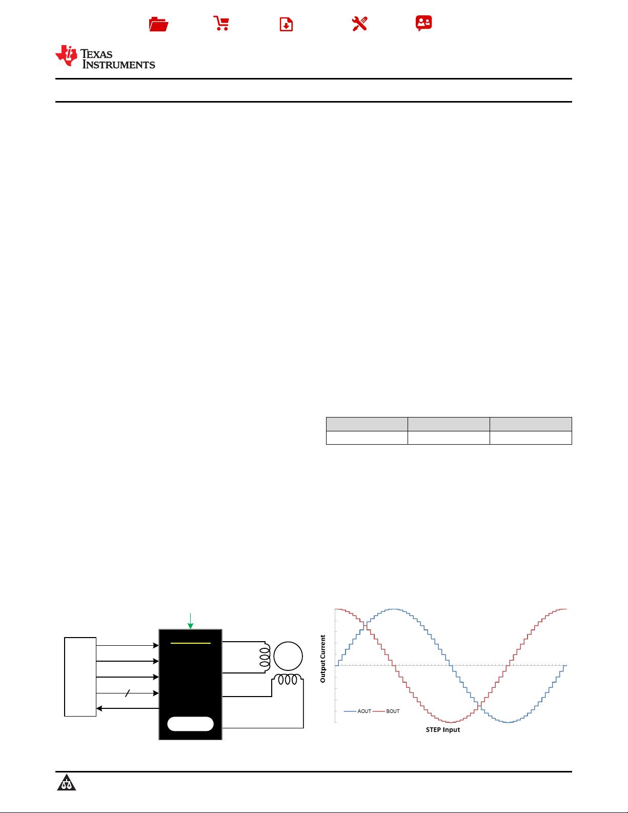
没有合适的资源?快使用搜索试试~ 我知道了~
首页DRV8825电机驱动芯片数据手册
资源详情
资源评论
资源推荐
STEP
Step Size
Decay Mode
8.2 to 45 V
Controller
M
+ -
+ -
DRV8825
1/32 µstep
Stepper
Motor Driver
2.5 A
2.5 A
DIR
nFAULT
Product
Folder
Sample &
Buy
Technical
Documents
Tools &
Software
Support &
Community
DRV8825
SLVSA73F –APRIL 2010–REVISED JULY 2014
DRV8825 Stepper Motor Controller IC
1 Features 3 Description
The DRV8825 provides an integrated motor driver
1
• PWM Microstepping Stepper Motor Driver
solution for printers, scanners, and other automated
– Built-In Microstepping Indexer
equipment applications. The device has two H-bridge
– Up to 1/32 Microstepping
drivers and a microstepping indexer, and is intended
to drive a bipolar stepper motor. The output driver
• Multiple Decay Modes
block consists of N-channel power MOSFET’s
– Mixed Decay
configured as full H-bridges to drive the motor
– Slow Decay
windings. The DRV8825 is capable of driving up to
2.5 A of current from each output (with proper heat
– Fast Decay
sinking, at 24 V and 25°C).
• 8.2-V to 45-V Operating Supply Voltage Range
A simple STEP/DIR interface allows easy interfacing
• 2.5-A Maximum Drive Current at 24 V and
to controller circuits. Mode pins allow for configuration
T
A
= 25°C
of the motor in full-step up to 1/32-step modes. Decay
• Simple STEP/DIR Interface
mode is configurable so that slow decay, fast decay,
• Low Current Sleep Mode
or mixed decay can be used. A low-power sleep
mode is provided which shuts down internal circuitry
• Built-In 3.3-V Reference Output
to achieve very low quiescent current draw. This
• Small Package and Footprint
sleep mode can be set using a dedicated nSLEEP
• Protection Features
pin.
– Overcurrent Protection (OCP)
Internal shutdown functions are provided for
– Thermal Shutdown (TSD)
overcurrent, short circuit, under voltage lockout and
over temperature. Fault conditions are indicated via
– VM Undervoltage Lockout (UVLO)
the nFAULT pin.
– Fault Condition Indication Pin (nFAULT)
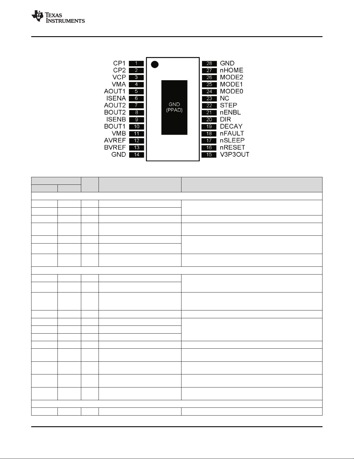
Device Information
(1)
2 Applications
PART NUMBER PACKAGE BODY SIZE (NOM)
• Automatic Teller Machines
DRV8825 HTSSOP (28) 9.70 mm × 6.40 mm
• Money Handling Machines
(1) For all available packages, see the orderable addendum at
• Video Security Cameras the end of the data sheet.
• Printers
• Scanners
• Office Automation Machines
• Gaming Machines
• Factory Automation
• Robotics
4 Simplified Schematic
Microstepping Current Waveform
1
An IMPORTANT NOTICE at the end of this data sheet addresses availability, warranty, changes, use in safety-critical applications,
intellectual property matters and other important disclaimers. PRODUCTION DATA.
DRV8825
SLVSA73F –APRIL 2010–REVISED JULY 2014
www.ti.com
Table of Contents
8.3 Feature Description................................................. 11
1 Features.................................................................. 1
8.4 Device Functional Modes........................................ 17
2 Applications ........................................................... 1
9 Application and Implementation ........................ 18
3 Description ............................................................. 1
9.1 Application Information............................................ 18
4 Simplified Schematic............................................. 1
9.2 Typical Application ................................................. 18
5 Revision History..................................................... 2
10 Power Supply Recommendations ..................... 21
6 Pin Configuration and Functions......................... 3
10.1 Bulk Capacitance .................................................. 21
7 Specifications......................................................... 4
10.2 Power Supply and Logic Sequencing ................... 21
7.1 Absolute Maximum Ratings ...................................... 4
11 Layout................................................................... 22
7.2 Handling Ratings....................................................... 4
11.1 Layout Guidelines ................................................. 22
7.3 Recommended Operating Conditions....................... 4
11.2 Layout Example .................................................... 22
7.4 Thermal Information.................................................. 5
11.3 Thermal Protection................................................ 22
7.5 Electrical Characteristics........................................... 6
12 Device and Documentation Support ................. 24
7.6 Timing Requirements................................................ 7
12.1 Trademarks........................................................... 24
7.7 Typical Characteristics.............................................. 8
12.2 Electrostatic Discharge Caution............................ 24
8 Detailed Description .............................................. 9
12.3 Glossary................................................................ 24
8.1 Overview ................................................................... 9
13 Mechanical, Packaging, and Orderable
8.2 Functional Block Diagram ....................................... 10
Information ........................................................... 24
5 Revision History
Changes from Revision E (August 2013) to Revision F Page
• Added new sections and reordered data sheet to fit new TI flow .......................................................................................... 1
• Updated pin descriptions ....................................................................................................................................................... 3
• Added power supply ramp rate and updated ISENSEx pin voltage in Absolute Maximum Ratings ..................................... 4
• Updated V
IL
voltage minimum and typical in Electrical Characteristics ................................................................................. 6
• Updated I
IN
and t
DEG
in Electrical Characteristics .................................................................................................................. 6
2 Submit Documentation Feedback Copyright © 2010–2014, Texas Instruments Incorporated
Product Folder Links: DRV8825
DRV8825
www.ti.com
SLVSA73F –APRIL 2010–REVISED JULY 2014
6 Pin Configuration and Functions
Pin Functions
PIN
EXTERNAL COMPONENTS
I/O
(1)
DESCRIPTION
OR CONNECTIONS
NAME NO.
POWER AND GROUND
CP1 1 I/O Charge pump flying capacitor
Connect a 0.01-μF 50-V capacitor between CP1 and CP2.
CP2 2 I/O Charge pump flying capacitor
GND 14, 28 — Device ground
Connect a 0.1-μF 16-V ceramic capacitor and a 1-MΩ resistor to
VCP 3 I/O High-side gate drive voltage
VM.
VMA 4 — Bridge A power supply Connect to motor supply (8.2 to 45 V). Both pins must be
connected to the same supply, bypassed with a 0.1-µF capacitor
VMB 11 — Bridge B power supply
to GND, and connected to appropriate bulk capacitance.
Bypass to GND with a 0.47-μF 6.3-V ceramic capacitor. Can be
V3P3OUT 15 O 3.3-V regulator output
used to supply VREF.
CONTROL
AVREF 12 I Bridge A current set reference input Reference voltage for winding current set. Normally AVREF and
BVREF are connected to the same voltage. Can be connected to
BVREF 13 I Bridge B current set reference input
V3P3OUT.
Low = slow decay, open = mixed decay,
DECAY 19 I Decay mode high = fast decay.
Internal pulldown and pullup.
DIR 20 I Direction input Level sets the direction of stepping. Internal pulldown.
MODE0 24 I Microstep mode 0
MODE0 through MODE2 set the step mode - full, 1/2, 1/4, 1/8/
MODE1 25 I Microstep mode 1
1/16, or 1/32 step. Internal pulldown.
MODE2 26 I Microstep mode 2
NC 23 — No connect Leave this pin unconnected.
Logic high to disable device outputs and indexer operation, logic
nENBL 21 I Enable input
low to enable. Internal pulldown.
Active-low reset input initializes the indexer logic and disables the
nRESET 16 I Reset input
H-bridge outputs. Internal pulldown.
Logic high to enable device, logic low to enter low-power sleep
nSLEEP 17 I Sleep mode input
mode. Internal pulldown.
Rising edge causes the indexer to move one step. Internal
STEP 22 I Step input
pulldown.
STATUS
nFAULT 18 OD Fault Logic low when in fault condition (overtemp, overcurrent)
(1) Directions: I = input, O = output, OD = open-drain output, IO = input/output
Copyright © 2010–2014, Texas Instruments Incorporated Submit Documentation Feedback 3
Product Folder Links: DRV8825
DRV8825
SLVSA73F –APRIL 2010–REVISED JULY 2014
www.ti.com
Pin Functions (continued)
PIN
EXTERNAL COMPONENTS
I/O
(1)
DESCRIPTION
OR CONNECTIONS
NAME NO.
nHOME 27 OD Home position Logic low when at home state of step table
OUTPUT
AOUT1 5 O Bridge A output 1
Connect to bipolar stepper motor winding A.
Positive current is AOUT1 → AOUT2
AOUT2 7 O Bridge A output 2
BOUT1 10 O Bridge B output 1
Connect to bipolar stepper motor winding B.
Positive current is BOUT1 → BOUT2
BOUT2 8 O Bridge B output 2
ISENA 6 I/O Bridge A ground / Isense Connect to current sense resistor for bridge A.
ISENB 9 I/O Bridge B ground / Isense Connect to current sense resistor for bridge B.
7 Specifications
7.1 Absolute Maximum Ratings
(1)(2)
MIN MAX UNIT
Power supply voltage –0.3 47 V
V
(VMx)
Power supply ramp rate 1 V/µs
Digital pin voltage –0.5 7 V
V
(xVREF)
Input voltage –0.3 4 V
ISENSEx pin voltage
(3)
–0.8 0.8 V
Peak motor drive output current, t < 1 μs Internally limited A
Continuous motor drive output current
(4)
0 2.5 A
Continuous total power dissipation See Thermal Information
T
J
Operating junction temperature range –40 150 °C
(1) Stresses beyond those listed under Absolute Maximum Ratings may cause permanent damage to the device. These are stress ratings
only, and functional operation of the device at these or any other conditions beyond those indicated under Recommended Operating
Conditions is not implied. Exposure to absolute-maximum-rated conditions for extended periods may affect device reliability.
(2) All voltage values are with respect to network ground terminal.
(3) Transients of ± 1 V for less than 25 ns are acceptable
(4) Power dissipation and thermal limits must be observed.
7.2 Handling Ratings
MIN MAX UNIT
T
stg
Storage temperature range –60 150 °C
Human body model (HBM), per ANSI/ESDA/JEDEC JS-001, all pins
(1)
–2000 2000
Electrostatic
V
(ESD)
V
discharge
Charged device model (CDM), per JEDEC specification JESD22-C101, all pins
(2)
–500 500
(1) JEDEC document JEP155 states that 500-V HBM allows safe manufacturing with a standard ESD control process.
(2) JEDEC document JEP157 states that 250-V CDM allows safe manufacturing with a standard ESD control process.
7.3 Recommended Operating Conditions
MIN NOM MAX UNIT
V
(VMx)
Motor power supply voltage range
(1)
8.2 45 V
V
(VREF)
VREF input voltage
(2)
1 3.5 V
I
V3P3
V3P3OUT load current 0 1 mA
(1) All V
M
pins must be connected to the same supply voltage.
(2) Operational at VREF between 0 to 1 V, but accuracy is degraded.
4 Submit Documentation Feedback Copyright © 2010–2014, Texas Instruments Incorporated
Product Folder Links: DRV8825
DRV8825
www.ti.com
SLVSA73F –APRIL 2010–REVISED JULY 2014
7.4 Thermal Information
DRV8825
THERMAL METRIC
(1)
PWP UNIT
28 PINS
R
θJA
Junction-to-ambient thermal resistance
(2)
31.6
R
θJC(top)
Junction-to-case (top) thermal resistance
(3)
15.9
R
θJB
Junction-to-board thermal resistance
(4)
5.6
°C/W
ψ
JT
Junction-to-top characterization parameter
(5)
0.2
ψ
JB
Junction-to-board characterization parameter
(6)
5.5
R
θJC(bot)
Junction-to-case (bottom) thermal resistance
(7)
1.4
(1) For more information about traditional and new thermal metrics, see the IC Package Thermal Metrics application report, SPRA953.
(2) The junction-to-ambient thermal resistance under natural convection is obtained in a simulation on a JEDEC-standard, high-K board, as
specified in JESD51-7, in an environment described in JESD51-2a.
(3) The junction-to-case (top) thermal resistance is obtained by simulating a cold plate test on the package top. No specific JEDEC-
standard test exists, but a close description can be found in the ANSI SEMI standard G30-88.
(4) The junction-to-board thermal resistance is obtained by simulating in an environment with a ring cold plate fixture to control the PCB
temperature, as described in JESD51-8.
(5) The junction-to-top characterization parameter, ψ
JT
, estimates the junction temperature of a device in a real system and is extracted
from the simulation data for obtaining θ
JA
, using a procedure described in JESD51-2a (sections 6 and 7).
(6) The junction-to-board characterization parameter, ψ
JB
, estimates the junction temperature of a device in a real system and is extracted
from the simulation data for obtaining θ
JA
, using a procedure described in JESD51-2a (sections 6 and 7).
(7) The junction-to-case (bottom) thermal resistance is obtained by simulating a cold plate test on the exposed (power) pad. No specific
JEDEC standard test exists, but a close description can be found in the ANSI SEMI standard G30-88.
Spacer
Copyright © 2010–2014, Texas Instruments Incorporated Submit Documentation Feedback 5
Product Folder Links: DRV8825
剩余31页未读,继续阅读
沙滩黑大葱
- 粉丝: 8
- 资源: 4
上传资源 快速赚钱
- 我的内容管理 收起
- 我的资源 快来上传第一个资源
- 我的收益 登录查看自己的收益
- 我的积分 登录查看自己的积分
- 我的C币 登录后查看C币余额
- 我的收藏
- 我的下载
- 下载帮助
会员权益专享
最新资源
- RTL8188FU-Linux-v5.7.4.2-36687.20200602.tar(20765).gz
- c++校园超市商品信息管理系统课程设计说明书(含源代码) (2).pdf
- 建筑供配电系统相关课件.pptx
- 企业管理规章制度及管理模式.doc
- vb打开摄像头.doc
- 云计算-可信计算中认证协议改进方案.pdf
- [详细完整版]单片机编程4.ppt
- c语言常用算法.pdf
- c++经典程序代码大全.pdf
- 单片机数字时钟资料.doc
- 11项目管理前沿1.0.pptx
- 基于ssm的“魅力”繁峙宣传网站的设计与实现论文.doc
- 智慧交通综合解决方案.pptx
- 建筑防潮设计-PowerPointPresentati.pptx
- SPC统计过程控制程序.pptx
- SPC统计方法基础知识.pptx
资源上传下载、课程学习等过程中有任何疑问或建议,欢迎提出宝贵意见哦~我们会及时处理!
点击此处反馈
安全验证
文档复制为VIP权益,开通VIP直接复制
信息提交成功
评论0