没有合适的资源?快使用搜索试试~ 我知道了~
首页EP1C6Q240C8 开发板资料
EP1C6Q240C8 开发板资料
5星 · 超过95%的资源 需积分: 10 51 下载量 200 浏览量
更新于2023-03-03
评论 1
收藏 584KB PDF 举报
EP1C6Q240C8 开发板资料EP1C6Q240C8 开发板资料EP1C6Q240C8 开发板资料
资源详情
资源评论
资源推荐
®
Altera Corporation 1
Cyclone
FPGA Family
March 2003, ver. 1.1 Data Sheet
DS-CYCLONE-1.1
Introduction
Preliminary
Information
The Cyclone
TM
field programmable gate array family is based on a 1.5-V,
0.13-µm, all-layer copper SRAM process, with densities up to 20,060 logic
elements (LEs) and up to 288 Kbits of RAM. With features like phase-
locked loops (PLLs) for clocking and a dedicated double data rate (DDR)
interface to meet DDR SDRAM and fast cycle RAM (FCRAM) memory
requirements, Cyclone devices are a cost-effective solution for data-path
applications. Cyclone devices support various I/O standards, including
LVDS at data rates up to 311 megabits per second (Mbps) and 66-MHz,
32-bit peripheral component interconnect (PCI), for interfacing with and
supporting ASSP and ASIC devices. Altera also offers new low-cost serial
configuration devices to configure Cyclone devices.
Features...
■ 2,910 to 20,060 LEs, see Table 1
■ Up to 294,912 RAM bits (36,864 bytes)
■ Supports configuration through low-cost serial configuration device
■ Support for LVTTL, LVCMOS, SSTL-2, and SSTL-3 I/O standards
■ Support for 66-MHz, 32-bit PCI standard
■ Low speed (311 Mbps) LVDS I/O support
■ Up to two PLLs per device provide clock multiplication and phase
shifting
■ Up to eight global clock lines with six clock resources available per
logic array block (LAB) row
■ Support for external memory, including DDR SDRAM (133 MHz),
FCRAM, and single data rate (SDR) SDRAM
■ Support for multiple intellectual property (IP) cores, including
Altera
MegaCore
functions and Altera Megafunctions Partners
Program (AMPP
SM
) megafunctions
Note to Table 1:
(1) This parameter includes global clock pins.
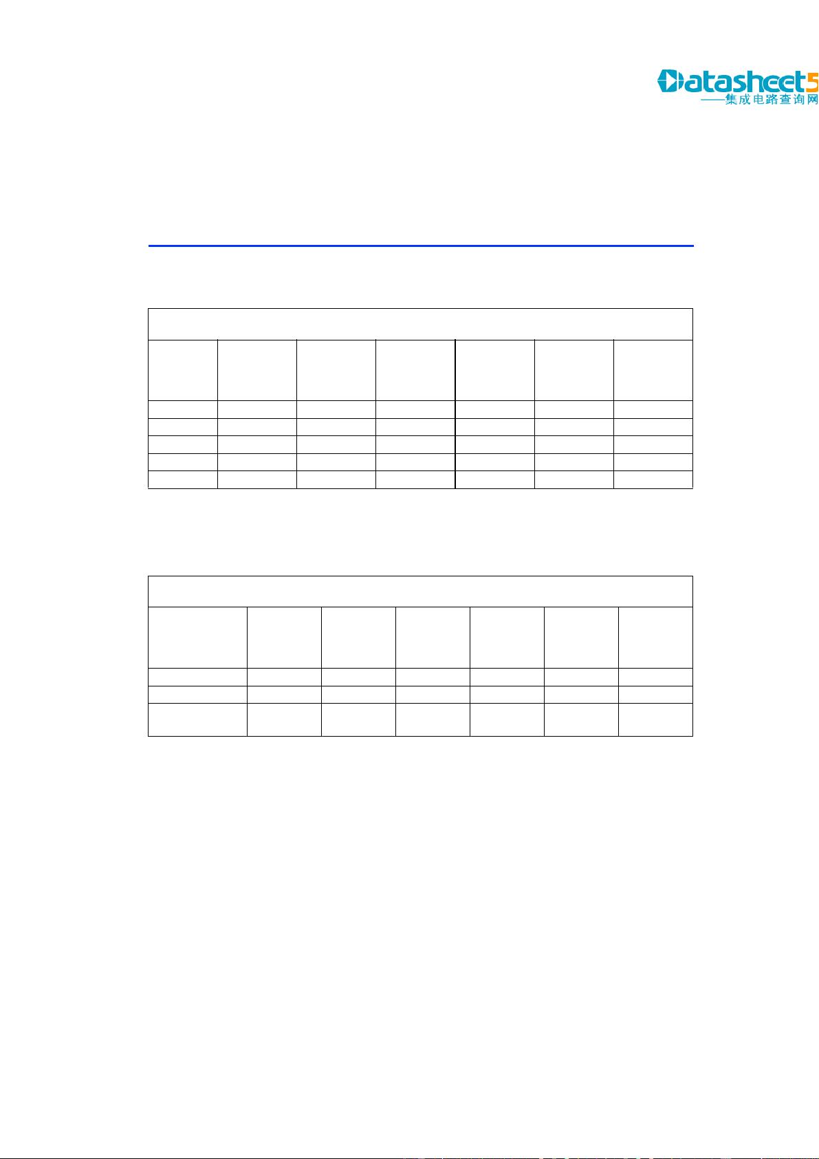
Table 1. Cyclone Device Features
Feature EP1C3 EP1C4 EP1C6 EP1C12 EP1C20
LEs 2,910 4,000 5,980 12,060 20,060
M4K RAM blocks (128 × 36bits)1317205264
Total RAM bits 59,904 78,336 92,160 239,616 294,912
PLLs 12222
Maximum user I/O pins (1) 104 301 185 249 301
2 Altera Corporation
Cyclone FPGA Family Data Sheet Preliminary Information
Cyclone devices are available in quad flat pack (QFP) and space-saving
FineLine BGA
packages (see Tables 2 through 3).
Notes to Table 2:
(1) TQFP: thin quad flat pack.
PQFP: plastic quad flat pack.
(2) Cyclone devices support vertical migration within the same package (i.e., designers can migrate between the EP1C3
device in the 144-pin TQFP package and the EP1C6 device in the same package).
Table 2. Cyclone Package Options & I/O Pin Counts
Device 100-Pin
TQFP (1)
144-Pin
TQFP (1), (2)
240-Pin
PQFP (1)
256-Pin
FineLine
BGA
324-Pin
FineLine
BGA
400-Pin
FineLine
BGA
EP1C3 65 104
EP1C4 249 301
EP1C6 98 185 185
EP1C12 173 185 249
EP1C20 233 301
Table 3. Cyclone QFP & FineLine BGA Package Sizes
Dimension 100-Pin
TQFP
144-Pin
TQFP
240-Pin
PQFP
256-Pin
FineLine
BGA
324-Pin
FineLine
BGA
400-Pin
FineLine
BGA
Pitch (mm) 0.5 0.5 0.5 1.0 1.0 1.0
Area (mm
2
) 256 484 1,024 289 361 441
Length × width
(mm × mm)
16 × 16 22 × 22 34.6 × 34.6 17 × 17 19 × 19 21 × 21
Altera Corporation 3
Preliminary Information Cyclone FPGA Family Data Sheet
Table of
Contents
Introduction........................................................................................................1
Features ...............................................................................................................1
Table of Contents ...............................................................................................3
Functional Description......................................................................................4
Logic Array Blocks.............................................................................................6
Logic Elements ...................................................................................................9
MultiTrack Interconnect .................................................................................17
Embedded Memory.........................................................................................23
Global Clock Network & Phase-Locked Loops...........................................34
I/O Structure....................................................................................................44
Power Sequencing & Hot Socketing .............................................................60
IEEE Std. 1149.1 (JTAG) Boundary Scan Support.......................................60
SignalTap II Embedded Logic Analyzer ......................................................65
Configuration ...................................................................................................65
Operating Conditions......................................................................................67
Power Consumption........................................................................................73
Timing Model...................................................................................................73
Software.............................................................................................................93
Device Pin-Outs ...............................................................................................93
Ordering Information......................................................................................93
4 Altera Corporation
Cyclone FPGA Family Data Sheet Preliminary Information
Functional
Description
Cyclone devices contain a two-dimensional row- and column-based
architecture to implement custom logic. Column and row interconnects of
varying speeds provide signal interconnects between LABs and
embedded memory blocks.
The logic array consists of LABs, with 10 LEs in each LAB. An LE is a small
unit of logic providing efficient implementation of user logic functions.
LABs are grouped into rows and columns across the device. Cyclone
devices range between 2,910 to 20,060 LEs.
M4K RAM blocks are true dual-port memory blocks with 4K bits of
memory plus parity (4,608 bits). These blocks provide dedicated true
dual-port, simple dual-port, or single-port memory up to 36-bits wide at
up to 200 MHz. These blocks are grouped into columns across the device
in between certain LABs. Cyclone devices offer between 60 to 288 Kbits of
embedded RAM.
Each Cyclone device I/O pin is fed by an I/O element (IOE) located at the
ends of LAB rows and columns around the periphery of the device. I/O
pins support various single-ended and differential I/O standards, such as
the 66-MHz, 32-bit PCI standard and the LVDS I/O standard at up to
311 Mbps. Each IOE contains a bidirectional I/O buffer and three registers
for registering input, output, and output-enable signals. Dual-purpose
DQS, DQ, and DM pins along with delay chains (used to phase-align DDR
signals) provide interface support with external memory devices such as
DDR SDRAM, and FCRAM devices at up to 133 MHz (266 Mbps).
Cyclone devices provide a global clock network and up to two PLLs. The
global clock network consists of eight global clock lines that drive
throughout the entire device. The global clock network can provide clocks
for all resources within the device, such as IOEs, LEs, and memory blocks.
The global clock lines can also be used for control signals. Cyclone PLLs
provide general-purpose clocking with clock multiplication and phase
shifting as well as external outputs for high-speed differential I/O
support.
Figure 1 shows a diagram of the Cyclone EP1C12 device.
Altera Corporation 5
Preliminary Information Cyclone FPGA Family Data Sheet
Figure 1. Cyclone EP1C12 Device Block Diagram
The number of M4K RAM blocks, PLLs, rows, and columns vary per
device. Table 4 lists the resources available in each Cyclone device.
Logic Array
PLL
IOEs
M4K Blocks
EP1C12 Device
Table 4. Cyclone Device Resources
Device M4K RAM PLLs LAB Columns LAB Rows
Columns Blocks
EP1C3 1 13 1 24 13
EP1C4 1 17 2 26 17
EP1C6 1 20 2 32 20
EP1C12 2 52 2 48 26
EP1C20 2 64 2 64 32
剩余94页未读,继续阅读
普通网友
- 粉丝: 4
- 资源: 15
上传资源 快速赚钱
- 我的内容管理 收起
- 我的资源 快来上传第一个资源
- 我的收益 登录查看自己的收益
- 我的积分 登录查看自己的积分
- 我的C币 登录后查看C币余额
- 我的收藏
- 我的下载
- 下载帮助
会员权益专享
最新资源
- c++校园超市商品信息管理系统课程设计说明书(含源代码) (2).pdf
- 建筑供配电系统相关课件.pptx
- 企业管理规章制度及管理模式.doc
- vb打开摄像头.doc
- 云计算-可信计算中认证协议改进方案.pdf
- [详细完整版]单片机编程4.ppt
- c语言常用算法.pdf
- c++经典程序代码大全.pdf
- 单片机数字时钟资料.doc
- 11项目管理前沿1.0.pptx
- 基于ssm的“魅力”繁峙宣传网站的设计与实现论文.doc
- 智慧交通综合解决方案.pptx
- 建筑防潮设计-PowerPointPresentati.pptx
- SPC统计过程控制程序.pptx
- SPC统计方法基础知识.pptx
- MW全能培训汽轮机调节保安系统PPT教学课件.pptx
资源上传下载、课程学习等过程中有任何疑问或建议,欢迎提出宝贵意见哦~我们会及时处理!
点击此处反馈
安全验证
文档复制为VIP权益,开通VIP直接复制
信息提交成功
评论1