没有合适的资源?快使用搜索试试~ 我知道了~
首页LPC2119手册Single-chip 16/32-bit microcontrollers; 64/128/256 kB ISP/IAP
LPC2119的手册,有其原理图及其他的信息。希望对各位朋友有点帮助,我也是初学者,互相交流.The LPC2109/2119/2129 are based on a 16/32-bit ARM7TDMI-S CPU with real-time emulation and embedded trace support, together with 64/128/256 kB of embedded high-speed flash memory. A 128-bit wide memory interface and a unique accelerator architecture enable 32-bit code execution at maximum clock rate. For critical code size applications, the alternative 16-bit Thumb mode reduces code by more than 30 % with minimal performance penalty.
资源详情
资源评论
资源推荐
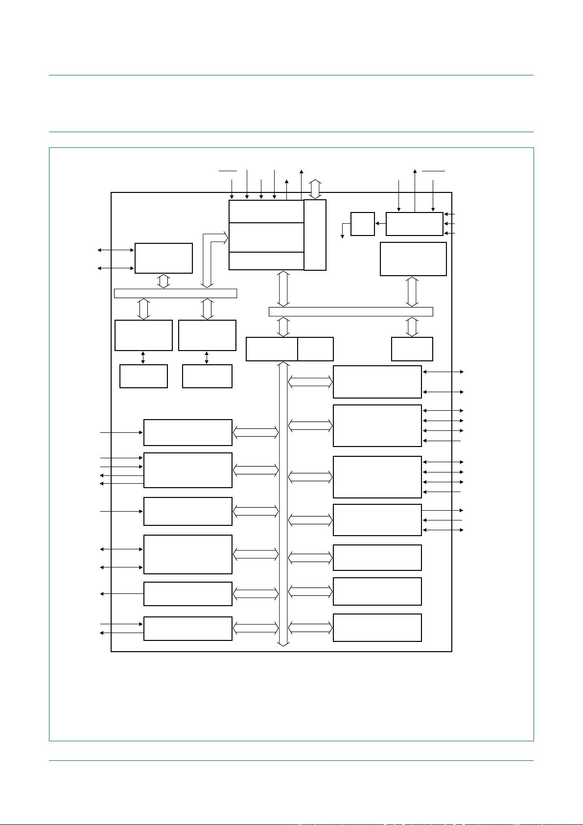
1. General description
The LPC2109/2119/2129 are based on a 16/32-bit ARM7TDMI-S CPU with real-time
emulation and embedded trace support, together with 64/128/256 kB of embedded
high-speed flash memory. A 128-bit wide memory interface and a unique accelerator
architecture enable 32-bit code execution at maximum clock rate. For critical code size
applications, the alternative 16-bit Thumb mode reduces code by more than 30 % with
minimal performance penalty.
With their compact 64-pin package, low power consumption, various 32-bit timers,
4-channel 10-bit ADC, two advanced CAN channels, PWM channels and 46 fast GPIO
lines with up to nine external interrupt pins these microcontrollers are particularly suitable
for automotive and industrial control applications, as well as medical systems and
fault-tolerant maintenance buses. With a wide range of additional serial communications
interfaces, they are also suited for communication gateways and protocol converters as
well as many other general-purpose applications.
Remark: Throughout the data sheet, the term LPC2109/2119/2129 will apply to devices
with and without the /00 or /01 suffixes. The /00 or the /01 suffix will be used to
differentiate from other devices only when necessary.
2. Features
2.1 Key features brought by LPC2109/2119/2129/01 devices
n Fast GPIO ports enable port pin toggling up to 3.5 times faster than the original device.
They also allow for a port pin to be read at any time regardless of its function.
n Dedicated result registers for ADC(s) reduce interrupt overhead. The ADC pads are
5 V tolerant when configured for digital I/O function(s).
n UART0/1 include fractional baud rate generator, auto-bauding capabilities and
handshake flow-control fully implemented in hardware.
n Buffered SSP serial controller supporting SPI, 4-wire SSI, and Microwire formats.
n SPI programmable data length and master mode enhancement.
n Diversified Code Read Protection (CRP) enables different security levels to be
implemented. This feature is available in LPC2109/2119/2129/00 devices as well.
n General purpose timers can operate as external event counters.
2.2 Key features common for all devices
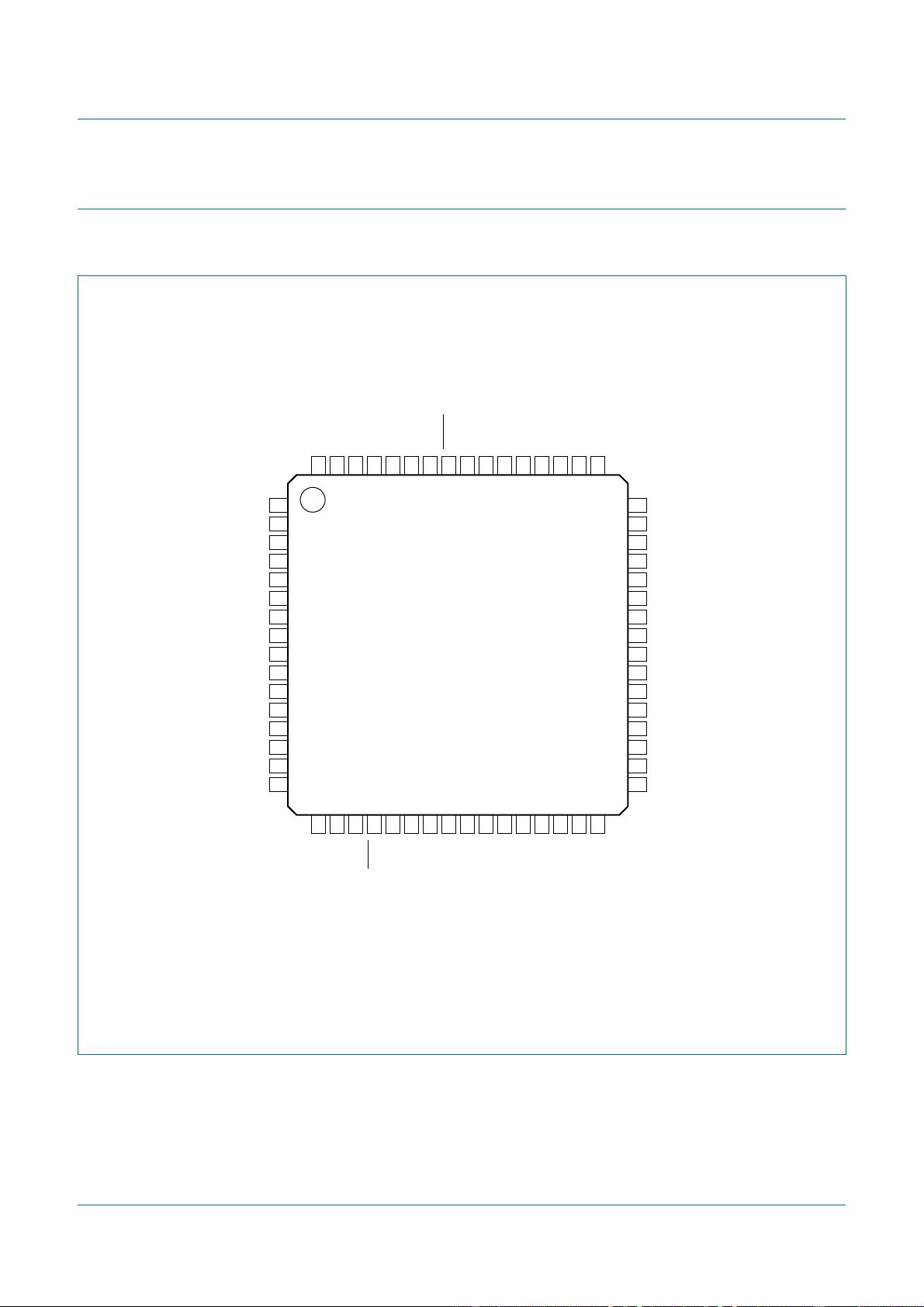
n 16/32-bit ARM7TDMI-S microcontroller in a tiny LQFP64 package.
n 8/16 kB on-chip static RAM.
LPC2109/2119/2129
Single-chip 16/32-bit microcontrollers; 64/128/256 kB ISP/IAP
flash with 10-bit ADC and CAN
Rev. 06 — 10 December 2007 Product data sheet
LPC2109_2119_2129_6 © NXP B.V. 2007. All rights reserved.
Product data sheet Rev. 06 — 10 December 2007 2 of 44
NXP Semiconductors
LPC2109/2119/2129
Single-chip 16/32-bit microcontrollers
n 64/128/256 kB on-chip flash program memory. 128-bit wide interface/accelerator
enables high speed 60 MHz operation.
n In-System Programming (ISP) and In-Application Programming (IAP) via on-chip
bootloader software. Flash programming takes 1 ms per 512 B line. Single sector or
full chip erase takes 400 ms.
n EmbeddedICE-RT interface enables breakpoints and watch points. Interrupt service
routines can continue to execute while the foreground task is debugged with the
on-chip RealMonitor software.
n Embedded Trace Macrocell (ETM) enables non-intrusive high speed real-time tracing
of instruction execution.
n Two interconnected CAN interfaces (one for LPC2109) with advanced acceptance
filters.
n Four-channel 10-bit A/D converter with conversion time as low as 2.44 µs.
n Multiple serial interfaces including two UARTs (16C550), Fast I
2
C-bus (400 kbit/s) and
two SPIs.
n 60 MHz maximum CPU clock available from programmable on-chip Phase-Locked
Loop with settling time of 100 µs.
n Vectored Interrupt Controller with configurable priorities and vector addresses.
n Two 32-bit timers (with four capture and four compare channels), PWM unit (six
outputs), Real-Time Clock (RTC) and watchdog.
n Up to forty-six 5 V tolerant general purpose I/O pins. Up to nine edge or level sensitive
external interrupt pins available.
n On-chip crystal oscillator with an operating range of 1 MHz to 30 MHz.
n Two low power modes, Idle and Power-down.
n Processor wake-up from Power-down mode via external interrupt.
n Individual enable/disable of peripheral functions for power optimization.
n Dual power supply:
u CPU operating voltage range of 1.65 V to 1.95 V (1.8 V ± 0.15 V).
u I/O power supply range of 3.0 V to 3.6 V (3.3 V ± 10 %) with 5 V tolerant I/O pads.
3. Ordering information
Table 1. Ordering information
Type number Package
Name Description Version
LPC2109FBD64/00 LQFP64 plastic low profile quad flat package; 64 leads;
body 10 × 10 × 1.4 mm
SOT314-2
LPC2109FBD64/01 LQFP64 plastic low profile quad flat package; 64 leads;
body 10 × 10 × 1.4 mm
SOT314-2
LPC2119FBD64 LQFP64 plastic low profile quad flat package; 64 leads;
body 10 × 10 × 1.4 mm
SOT314-2
LPC2119FBD64/00 LQFP64 plastic low profile quad flat package; 64 leads;
body 10 × 10 × 1.4 mm
SOT314-2
LPC2119FBD64/01 LQFP64 plastic low profile quad flat package; 64 leads;
body 10 × 10 × 1.4 mm
SOT314-2
LPC2109_2119_2129_6 © NXP B.V. 2007. All rights reserved.
Product data sheet Rev. 06 — 10 December 2007 3 of 44
NXP Semiconductors
LPC2109/2119/2129
Single-chip 16/32-bit microcontrollers
3.1 Ordering options
LPC2129FBD64 LQFP64 plastic low profile quad flat package; 64 leads;
body 10 × 10 × 1.4 mm
SOT314-2
LPC2129FBD64/00 LQFP64 plastic low profile quad flat package; 64 leads;
body 10 × 10 × 1.4 mm
SOT314-2
LPC2129FBD64/01 LQFP64 plastic low profile quad flat package; 64 leads;
body 10 × 10 × 1.4 mm
SOT314-2
Table 1. Ordering information
…continued
Type number Package
Name Description Version
Table 2. Ordering options
Type number Flash
memory
RAM CAN Fast GPIO/
SSP/
Enhanced
UART, ADC,
Timer
Temperature range
LPC2109FBD64/00 64 kB 8 kB 1 channel no −40 °C to +85 °C
LPC2109FBD64/01 64 kB 8 kB 1 channel yes −40 °C to +85 °C
LPC2119FBD64 128 kB 16 kB 2 channels no −40 °C to +85 °C
LPC2119FBD64/00 128 kB 16 kB 2 channels no −40 °C to +85 °C
LPC2119FBD64/01 128 kB 16 kB 2 channels yes −40 °C to +85 °C
LPC2129FBD64 256 kB 16 kB 2 channels no −40 °C to +85 °C
LPC2129FBD64/00 256 kB 16 kB 2 channels no −40 °C to +85 °C
LPC2129FBD64/01 256 kB 16 kB 2 channels yes −40 °C to +85 °C
LPC2109_2119_2129_6 © NXP B.V. 2007. All rights reserved.
Product data sheet Rev. 06 — 10 December 2007 4 of 44
NXP Semiconductors
LPC2109/2119/2129
Single-chip 16/32-bit microcontrollers
4. Block diagram
(1) Shared with GPIO.
(2) When test/debug interface is used, GPIO/other functions sharing these pins are not available.
(3) Only 1 for LPC2109.
(4) SSP interface and high-speed GPIO are available on LPC2109/01, LPC2119/01, and LPC2129/01 only.
Fig 1. Block diagram
SCL
(1)
P0[30:27],
P0[25:0]
TRST
(2)
TMS
(2)
TCK
(2)
TDI
(2)
TDO
(2)
XTAL2
XTAL1
SCK0
(1)
MOSI0
(1)
MISO0
(1)
EINT[3:0]
(1)
AIN[3:0]
(1)
SSEL0
(1)
RXD[1:0]
(1)
AHB BRIDGE
PLL
PWM0
ARM7TDMI-S
LPC2109
LPC2119
LPC2129
RESET
4 × CAP0
(1)
4 × CAP1
(1)
4 × MAT0
(1)
TD[2:1]
(1)
RD[2:1]
(1)
4 × MAT1
(1)
P1[31:16]
P0[30:27],
P0[25:0]
P1[31:16]
SDA
(1)
TXD[1:0]
(1)
DSR1
(1)
, CTS1
(1)
,
RTS1
(1)
, DTR1
(1)
,
DCD1
(1)
, RI1
(1)
RTCK
ARM7 LOCAL BUS
INTERNAL
SRAM
CONTROLLER
INTERNAL
FLASH
CONTROLLER
8/16 kB
SRAM
64/128/256 kB
FLASH
EXTERNAL
INTERRUPTS
CAPTURE/
COMPARE
TIMER 0/TIMER 1
A/D CONVERTER
GENERAL
PURPOSE I/O
CAN INTERFACE 1 AND 2
ACCEPTANCE FILTERS
(3)
TEST/DEBUG
INTERFACE
EMULATION TRACE
MODULE
AMBA Advanced High-performance
Bus (AHB)
system
clock
SYSTEM
FUNCTIONS
VECTORED
INTERRUPT
CONTROLLER
AHB
DECODER
I
2
C-BUS SERIAL
INTERFACE
AHB TO APB
BRIDGE
APB
DIVIDER
SPI0 SERIAL
INTERFACE
SCK1
(1)
MOSI1
(1)
MISO1
(1)
SSEL1
(1)
SPI1/SSP
(4)
SERIAL
INTERFACE
UART0/UART1
WATCHDOG
TIMER
SYSTEM
CONTROL
REAL-TIME CLOCK
002aad172
V
DD(3V3)
V
SS
V
DD(1V8)
PWM[6:1]
(1)
HIGH-SPEED
GPI/O
(4)
46 PINS TOTAL
LPC2109_2119_2129_6 © NXP B.V. 2007. All rights reserved.
Product data sheet Rev. 06 — 10 December 2007 5 of 44
NXP Semiconductors
LPC2109/2119/2129
Single-chip 16/32-bit microcontrollers
5. Pinning information
5.1 Pinning
(1) No TD2 and RD2 for LPC2109.
(2) Pin configuration is identical for devices with and without /00 and /01 suffixes.
Fig 2. Pin configuration
LPC2109
LPC2119
LPC2129
(2)
P0[21]/PWM5/CAP1[3] P1[20]/TRACESYNC
P0[22]/CAP0[0]/MAT0[0] P0[17]/CAP1[2]/SCK1/MAT1[2]
P0[23]/RD2
(1)
P0[16]/EINT0/MAT0[2]/CAP0[2]
P1[19]/TRACEPKT3 P0[15]/RI1/EINT2
P0[24]/TD2
(1)
P1[21]/PIPESTAT0
V
SS
V
DD(3V3)
V
DDA(3V3)
V
SS
P1[18]/TRACEPKT2 P0[14]/DCD1/EINT1
P0[25]/RD1 P1[22]/PIPESTAT1
TD1 P0[13]/DTR1/MAT1[1]
P0[27]/AIN0/CAP0[1]/MAT0[1] P0[12]/DSR1/MAT1[0]
P1[17]/TRACEPKT1 P0[11]/CTS1/CAP1[1]
P0[28]/AIN1/CAP0[2]/MAT0[2] P1[23]/PIPESTAT2
P0[29]/AIN2/CAP0[3]/MAT0[3] P0[10]/RTS1/CAP1[0]
P0[30]/AIN3/EINT3/CAP0[0] P0[9]/RXD1/PWM6/EINT3
P1[16]/TRACEPKT0 P0[8]/TXD1/PWM4
V
DD(1V8)
P1[27]/TDO
V
SS
V
DDA(1V8)
P0[0]/TXD0/PWM1 XTAL1
P1[31]/TRST XTAL2
P0[1]/RXD0/PWM3/EINT0 P1[28]/TDI
P0[2]/SCL/CAP0[0] V
SSA
V
DD(3V3)
V
SSA(PLL)
P1[26]/RTCK RESET
V
SS
P1[29]/TCK
P0[3]/SDA/MAT0[0]/EINT1 P0[20]/MAT1[3]/SSEL1/EINT3
P0[4]/SCK0/CAP0[1] P0[19]/MAT1[2]/MOSI1/CAP1[2]
P1[25]/EXTIN0 P0[18]/CAP1[3]/MISO1/MAT1[3]
P0[5]/MISO0/MAT0[1] P1[30]/TMS
P0[6]/MOSI0/CAP0.2 V
DD(3V3)
P0[7]/SSEL0/PWM2/EINT2 V
SS
P1[24]/TRACECLK V
DD(1V8)
002aad173
1
2
3
4
5
6
7
8
9
10
11
12
13
14
15
16
48
47
46
45
44
43
42
41
40
39
38
37
36
35
34
33
17
18
19
20
21
22
23
24
25
26
27
28
29
30
31
32
64
63
62
61
60
59
58
57
56
55
54
53
52
51
50
49
剩余43页未读,继续阅读
tianshuang2009
- 粉丝: 19
- 资源: 6
上传资源 快速赚钱
- 我的内容管理 收起
- 我的资源 快来上传第一个资源
- 我的收益 登录查看自己的收益
- 我的积分 登录查看自己的积分
- 我的C币 登录后查看C币余额
- 我的收藏
- 我的下载
- 下载帮助
会员权益专享
最新资源
- 2023年中国辣条食品行业创新及消费需求洞察报告.pptx
- 2023年半导体行业20强品牌.pptx
- 2023年全球电力行业评论.pptx
- 2023年全球网络安全现状-劳动力资源和网络运营的全球发展新态势.pptx
- 毕业设计-基于单片机的液体密度检测系统设计.doc
- 家用清扫机器人设计.doc
- 基于VB+数据库SQL的教师信息管理系统设计与实现 计算机专业设计范文模板参考资料.pdf
- 官塘驿林场林防火(资源监管)“空天地人”四位一体监测系统方案.doc
- 基于专利语义表征的技术预见方法及其应用.docx
- 浅谈电子商务的现状及发展趋势学习总结.doc
- 基于单片机的智能仓库温湿度控制系统 (2).pdf
- 基于SSM框架知识产权管理系统 (2).pdf
- 9年终工作总结新年计划PPT模板.pptx
- Hytera海能达CH04L01 说明书.pdf
- 数据中心运维操作标准及流程.pdf
- 报告模板 -成本分析与报告培训之三.pptx
资源上传下载、课程学习等过程中有任何疑问或建议,欢迎提出宝贵意见哦~我们会及时处理!
点击此处反馈
安全验证
文档复制为VIP权益,开通VIP直接复制
信息提交成功
评论0