

Application Report
SCAA062 – March 2003
1
DC-Coupling Between Differential LVPECL, LVDS, HSTL, and CM
Kal Mustafa / Chris Sterzik High Performance Analog
ABSTRACT
This report describes various methods of interfacing different logic levels. The focus is dc-
coupling between the following differential signaling: LVPECL (low-voltage positive-
referenced emitter coupled logic), LVDS (low-voltage differential signals), HSTL (high-
speed transceiver logic), and CML (current-mode logic). The report discusses sixteen
various interface cases between the aforementioned differential signaling levels.
Contents
1 AC-Coupling..................................................................................................................................2
1.1 LVPECL..................................................................................................................................3
1.2 LVDS ....................................................................................................................................7
1.3 CML ..................................................................................................................................11
1.4 HSTL ..................................................................................................................................13
2 References ..................................................................................................................................15
Figures
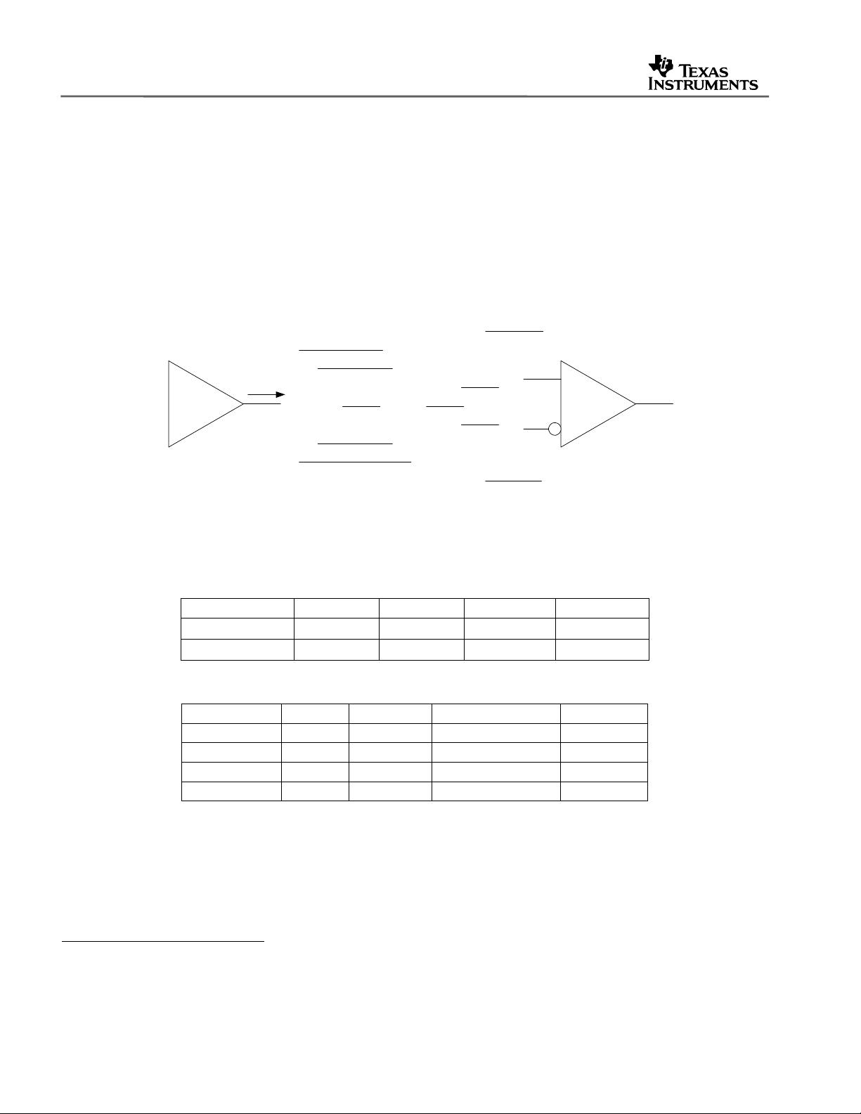
Figure 1. Input and Output Parameters..........................................................................................2
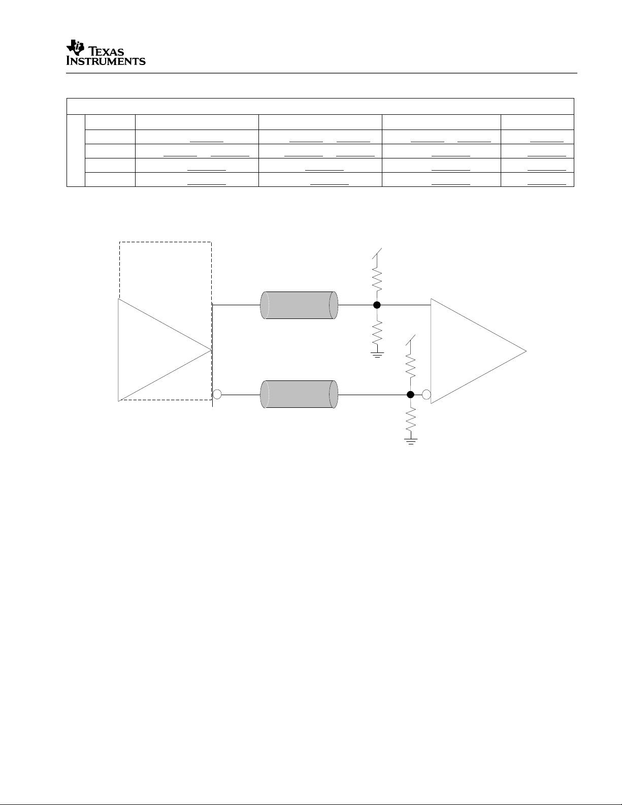
Figure 2. LVPECL to LVPECL..........................................................................................................3
Figure 3. LVPECL to LVPECL..........................................................................................................4
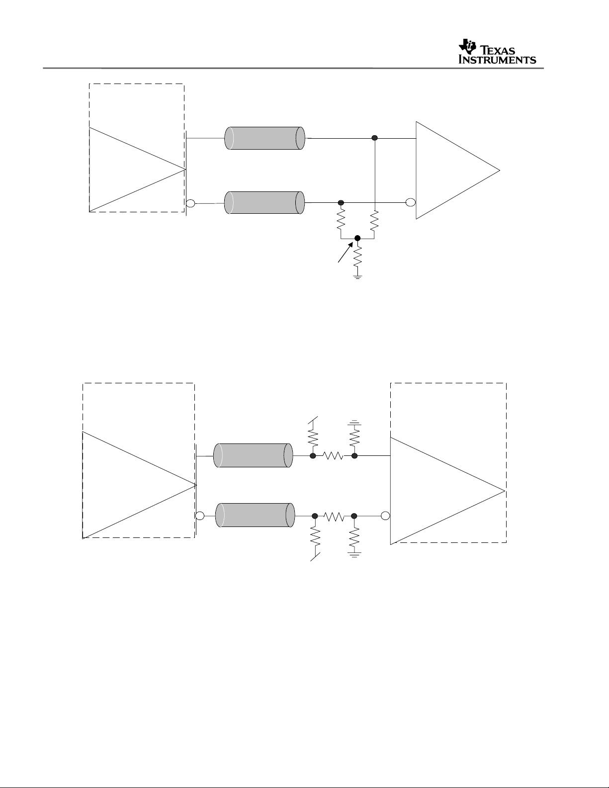
Figure 4. LVPECL to LVDS..............................................................................................................4
Figure 5. LVPECL to LVDS..............................................................................................................5
Figure 6. LVPECL to CML................................................................................................................5
Figure 7. LVPECL to CML Converter ..............................................................................................6
Figure 8. LVPECL to HSTL ..............................................................................................................6
Figure 9. LVDS to LVPECL..............................................................................................................7
Figure 10. LVDS to LVPECL..............................................................................................................8
Figure 11. LVDS to LVDS Without On-Chip Termination ................................................................8
Figure 12. LVDS to LVDS With On-Chip Termination......................................................................9
Figure 13. LVDS to CML Converter...................................................................................................9
Figure 14. LVDS to HSTL.................................................................................................................10
Figure 15. CML to LVPECL Translator............................................................................................11
Figure 16. CML to LVDS ..................................................................................................................11
Figure 17. CML to CML....................................................................................................................12
Figure 18. CML to HSTL...................................................................................................................13
Figure 19. HSTL to LVPECL Converter...........................................................................................13
Figure 20. HSTL to LVDS.................................................................................................................14
Figure 21. HSTL to CML Translator ................................................................................................14
Figure 22. HSTL to HSTL.................................................................................................................15
Tables
Table 1. Typical LVPECL, LVDS, HSTL, and CML Outputs..........................................................2
Table 2. Typical LVPECL, LVDS, CML, and HSTL Input Levels...................................................2
Table 3. Interface Table..................................................................................................................3
剩余15页未读,继续阅读

sfm1231
- 粉丝: 0
- 资源: 14
 我的内容管理
收起
我的内容管理
收起
- 我的资源
快来上传第一个资源
 我的收益 登录查看自己的收益
 我的积分
登录查看自己的积分
我的积分
登录查看自己的积分
 我的C币
登录后查看C币余额
我的C币
登录后查看C币余额
 我的收藏
我的收藏  我的下载
我的下载  下载帮助
下载帮助

会员权益专享


最新资源
- 2023年中国辣条食品行业创新及消费需求洞察报告.pptx
- 2023年半导体行业20强品牌.pptx
- 2023年全球电力行业评论.pptx
- 2023年全球网络安全现状-劳动力资源和网络运营的全球发展新态势.pptx
- 毕业设计-基于单片机的液体密度检测系统设计.doc
- 家用清扫机器人设计.doc
- 基于VB+数据库SQL的教师信息管理系统设计与实现 计算机专业设计范文模板参考资料.pdf
- 官塘驿林场林防火(资源监管)“空天地人”四位一体监测系统方案.doc
- 基于专利语义表征的技术预见方法及其应用.docx
- 浅谈电子商务的现状及发展趋势学习总结.doc
- 基于单片机的智能仓库温湿度控制系统 (2).pdf
- 基于SSM框架知识产权管理系统 (2).pdf
- 9年终工作总结新年计划PPT模板.pptx
- Hytera海能达CH04L01 说明书.pdf
- 数据中心运维操作标准及流程.pdf
- 报告模板 -成本分析与报告培训之三.pptx
资源上传下载、课程学习等过程中有任何疑问或建议,欢迎提出宝贵意见哦~我们会及时处理!
点击此处反馈


评论0