没有合适的资源?快使用搜索试试~ 我知道了~
首页 AT89S51芯片手册.pdf
AT89S51芯片手册.pdf
需积分: 50 10 下载量 108 浏览量
更新于2023-03-03
评论 1
收藏 488KB PDF 举报
AT89S51单片机的芯片手册 可使用,学习学习,做些小玩意 Features • Compatible with MCS®-51 Products • 4K Bytes of In-System Programmable (ISP) Flash Memory – Endurance: 10,000 Write/Erase Cycles • 4.0V to 5.5V Operating Range • Fully Static Operation: 0 Hz to 33 MHz • Three-level Program Memory Lock • 128 x 8-bit Internal RAM • 32 Programmable I/O Lines • Two 16-bit Timer/Counters • Six Interrupt Sources • Full Duplex UART Serial Channel • Low-power Idle and Power-down Modes • Interrupt Recovery from Power-down Mode • Watchdog Timer • Dual Data Pointer • Power-off Flag • Fast Programming Time • Flexible ISP Programming (Byte and Page Mode) • Green (Pb/Halide-free) Packaging Option
资源详情
资源评论
资源推荐
Features
• Compatible with MCS
®
-51
Products
• 4K Bytes of In-System Programmable (ISP) Flash Memory
– Endurance: 10,000 Write/Erase Cycles
• 4.0V to 5.5V Operating Range
• Fully Static Operation: 0 Hz to 33 MHz
• Three-level Program Memory Lock
• 128 x 8-bit Internal RAM
• 32 Programmable I/O Lines
• Two 16-bit Timer/Counters
• Six Interrupt Sources
• Full Duplex UART Serial Channel
• Low-power Idle and Power-down Modes
• Interrupt Recovery from Power-down Mode
• Watchdog Timer
• Dual Data Pointer
• Power-off Flag
• Fast Programming Time
• Flexible ISP Programming (Byte and Page Mode)
• Green (Pb/Halide-free) Packaging Option
1. Description
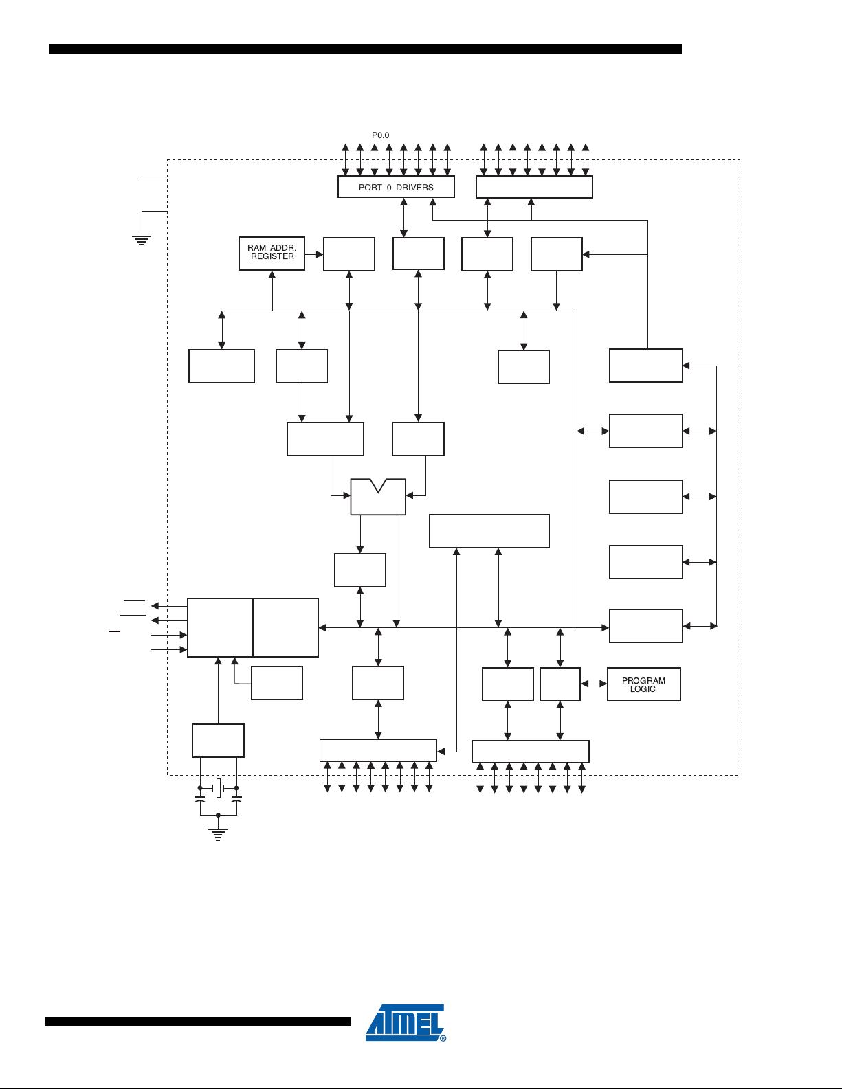
The AT89S51 is a low-power, high-performance CMOS 8-bit microcontroller with 4K
bytes of In-System Programmable Flash memory. The device is manufactured using
Atmel’s high-density nonvolatile memory technology and is compatible with the indus-
try-standard 80C51 instruction set and pinout. The on-chip Flash allows the program
memory to be reprogrammed in-system or by a conventional nonvolatile memory pro-
grammer. By combining a versatile 8-bit CPU with In-System Programmable Flash on
a monolithic chip, the Atmel AT89S51 is a powerful microcontroller which provides a
highly-flexible and cost-effective solution to many embedded control applications.
The AT89S51 provides the following standard features: 4K bytes of Flash, 128 bytes
of RAM, 32 I/O lines, Watchdog timer, two data pointers, two 16-bit timer/counters, a
five-vector two-level interrupt architecture, a full duplex serial port, on-chip oscillator,
and clock circuitry. In addition, the AT89S51 is designed with static logic for operation
down to zero frequency and supports two software selectable power saving modes.
The Idle Mode stops the CPU while allowing the RAM, timer/counters, serial port, and
interrupt system to continue functioning. The Power-down mode saves the RAM con-
tents but freezes the oscillator, disabling all other chip functions until the next external
interrupt or hardware reset.
8-bit
Microcontroller
with 4K Bytes
In-System
Programmable
Flash
AT89S51
2487D–MICRO–6/08
2
2487D–MICRO–6/08
AT89S51
2. Pin Configurations
2.1 40-lead PDIP
2.2 44-lead TQFP
1
2
3
4
5
6
7
8
9
10
11
12
13
14
15
16
17
18
19
20
40
39
38
37
36
35
34
33
32
31
30
29
28
27
26
25
24
23
22
21
P1.0
P1.1
P1.2
P1.3
P1.4
(MOSI) P1.5
(MISO) P1.6
(SCK) P1.7
RST
(RXD) P3.0
(TXD) P3.1
(INT0) P3.2
(INT1) P3.3
(T0) P3.4
(T1) P3.5
(WR) P3.6
(RD) P3.7
XTAL2
XTAL1
GND
VCC
P0.0 (AD0)
P0.1 (AD1)
P0.2 (AD2)
P0.3 (AD3)
P0.4 (AD4)
P0.5 (AD5)
P0.6 (AD6)
P0.7 (AD7)
EA/VPP
ALE/PROG
PSEN
P2.7 (A15)
P2.6 (A14)
P2.5 (A13)
P2.4 (A12)
P2.3 (A11)
P2.2 (A10)
P2.1 (A9)
P2.0 (A8)
1
2
3
4
5
6
7
8
9
10
11
33
32
31
30
29
28
27
26
25
24
23
44
43
42
41
40
39
38
37
36
35
34
12
13
14
15
16
17
18
19
20
21
22
(MOSI) P1.5
(MISO) P1.6
(SCK) P1.7
RST
(RXD) P3.0
NC
(TXD) P3.1
(INT0) P3.2
(INT1) P3.3
(T0) P3.4
(T1) P3.5
P0.4 (AD4)
P0.5 (AD5)
P0.6 (AD6)
P0.7 (AD7)
EA/VPP
NC
ALE/PROG
PSEN
P2.7 (A15)
P2.6 (A14)
P2.5 (A13)
P1.4
P1.3
P1.2
P1.1
P1.0
NC
VCC
P0.0 (AD0)
P0.1 (AD1)
P0.2 (AD2)
P0.3 (AD3)
(WR) P3.6
(RD) P3.7
XTAL2
XTAL1
GND
GND
(A8) P2.0
(A9) P2.1
(A10) P2.2
(A11) P2.3
(A12) P2.4
2.3 44-lead PLCC
7
8
9
10
11
12
13
14
15
16
17
39
38
37
36
35
34
33
32
31
30
29
(MOSI) P1.5
(MISO) P1.6
(SCK) P1.7
RST
(RXD) P3.0
NC
(TXD) P3.1
(INT0) P3.2
(INT1) P3.3
(T0) P3.4
(T1) P3.5
P0.4 (AD4)
P0.5 (AD5)
P0.6 (AD6)
P0.7 (AD7)
EA/VPP
NC
ALE/PROG
PSEN
P2.7 (A15)
P2.6 (A14)
P2.5 (A13)
6
5
4
3
2
1
44
43
42
41
40
18
19
20
21
22
23
24
25
26
27
28
(WR) P3.6
(RD) P3.7
XTAL2
XTAL1
GND
NC
(A8) P2.0
(A9) P2.1
(A10) P2.2
(A11) P2.3
(A12) P2.4
P1.4
P1.3
P1.2
P1.1
P1.0
NC
VCC
P0.0 (AD0)
P0.1 (AD1)
P0.2 (AD2)
P0.3 (AD3)
3
2487D–MICRO–6/08
AT89S51
3. Block Diagram
PORT 2 DRIVERS
PORT 2
LATCH
P2.0 - P2.7
FLASH
PORT 0
LATCH
RAM
PROGRAM
ADDRESS
REGISTER
BUFFER
PC
INCREMENTER
PROGRAM
COUNTER
DUAL DPTR
INSTRUCTION
REGISTER
B
REGISTER
INTERRUPT, SERIAL PORT,
AND TIMER BLOCKS
STACK
POINTER
ACC
TMP2 TMP1
ALU
PSW
TIMING
AND
CONTROL
PORT 1 DRIVERS
P1.0 - P1.7
PORT 3
LATCH
PORT 3 DRIVERS
P3.0 - P3.7
OSC
GND
V
CC
PSEN
ALE/PROG
EA / V
PP
RST
RAM ADDR.
REGISTER
PORT 0 DRIVERS
P0.0 - P0.7
PORT 1
LATCH
WATCH
DOG
ISP
PORT
PROGRAM
LOGIC
4
2487D–MICRO–6/08
AT89S51
4. Pin Description
4.1 VCC
Supply voltage.
4.2 GND
Ground.
4.3 Port 0
Port 0 is an 8-bit open drain bi-directional I/O port. As an output port, each pin can sink eight TTL
inputs. When 1s are written to port 0 pins, the pins can be used as high-impedance inputs.
Port 0 can also be configured to be the multiplexed low-order address/data bus during accesses
to external program and data memory. In this mode, P0 has internal pull-ups.
Port 0 also receives the code bytes during Flash programming and outputs the code bytes dur-
ing program verification. External pull-ups are required during program verification.
4.4 Port 1
Port 1 is an 8-bit bi-directional I/O port with internal pull-ups. The Port 1 output buffers can
sink/source four TTL inputs. When 1s are written to Port 1 pins, they are pulled high by the inter-
nal pull-ups and can be used as inputs. As inputs, Port 1 pins that are externally being pulled low
will source current (I
IL
) because of the internal pull-ups.
Port 1 also receives the low-order address bytes during Flash programming and verification.
4.5 Port 2
Port 2 is an 8-bit bi-directional I/O port with internal pull-ups. The Port 2 output buffers can
sink/source four TTL inputs. When 1s are written to Port 2 pins, they are pulled high by the inter-
nal pull-ups and can be used as inputs. As inputs, Port 2 pins that are externally being pulled low
will source current (I
IL
) because of the internal pull-ups.
Port 2 emits the high-order address byte during fetches from external program memory and dur-
ing accesses to external data memory that use 16-bit addresses (MOVX @ DPTR). In this
application, Port 2 uses strong internal pull-ups when emitting 1s. During accesses to external
data memory that use 8-bit addresses (MOVX @ RI), Port 2 emits the contents of the P2 Special
Function Register.
Port 2 also receives the high-order address bits and some control signals during Flash program-
ming and verification.
4.6 Port 3
Port 3 is an 8-bit bi-directional I/O port with internal pull-ups. The Port 3 output buffers can
sink/source four TTL inputs. When 1s are written to Port 3 pins, they are pulled high by the inter-
Port Pin Alternate Functions
P1.5 MOSI (used for In-System Programming)
P1.6 MISO (used for In-System Programming)
P1.7 SCK (used for In-System Programming)
5
2487D–MICRO–6/08
AT89S51
nal pull-ups and can be used as inputs. As inputs, Port 3 pins that are externally being pulled low
will source current (I
IL
) because of the pull-ups.
Port 3 receives some control signals for Flash programming and verification.
Port 3 also serves the functions of various special features of the AT89S51, as shown in the fol-
lowing table.
4.7 RST
Reset input. A high on this pin for two machine cycles while the oscillator is running resets
the device. This pin drives High for 98 oscillator periods after the Watchdog times out. The DIS-
RTO bit in SFR AUXR (address 8EH) can be used to disable this feature. In the default state of
bit DISRTO, the RESET HIGH out feature is enabled.
4.8 ALE/PROG
Address Latch Enable (ALE) is an output pulse for latching the low byte of the address during
accesses to external memory. This pin is also the program pulse input (PROG
) during Flash
programming.
In normal operation, ALE is emitted at a constant rate of 1/6 the oscillator frequency and may be
used for external timing or clocking purposes. Note, however, that one ALE pulse is skipped dur-
ing each access to external data memory.
If desired, ALE operation can be disabled by setting bit 0 of SFR location 8EH. With the bit set,
ALE is active only during a MOVX or MOVC instruction. Otherwise, the pin is weakly pulled high.
Setting the ALE-disable bit has no effect if the microcontroller is in external execution mode.
4.9 PSEN
Program Store Enable (PSEN) is the read strobe to external program memory.
When the AT89S51 is executing code from external program memory, PSEN
is activated twice
each machine cycle, except that two PSEN
activations are skipped during each access to exter-
nal data memory.
4.10 EA/VPP
External Access Enable. EA must be strapped to GND in order to enable the device to fetch
code from external program memory locations starting at 0000H up to FFFFH. Note, however,
that if lock bit 1 is programmed, EA
will be internally latched on reset.
Port Pin Alternate Functions
P3.0 RXD (serial input port)
P3.1 TXD (serial output port)
P3.2 INT0
(external interrupt 0)
P3.3 INT1
(external interrupt 1)
P3.4 T0 (timer 0 external input)
P3.5 T1 (timer 1 external input)
P3.6 WR
(external data memory write strobe)
P3.7 RD
(external data memory read strobe)
剩余30页未读,继续阅读
派狼不派
- 粉丝: 13
- 资源: 5
上传资源 快速赚钱
- 我的内容管理 收起
- 我的资源 快来上传第一个资源
- 我的收益 登录查看自己的收益
- 我的积分 登录查看自己的积分
- 我的C币 登录后查看C币余额
- 我的收藏
- 我的下载
- 下载帮助
会员权益专享
最新资源
- stc12c5a60s2 例程
- Android通过全局变量传递数据
- c++校园超市商品信息管理系统课程设计说明书(含源代码) (2).pdf
- 建筑供配电系统相关课件.pptx
- 企业管理规章制度及管理模式.doc
- vb打开摄像头.doc
- 云计算-可信计算中认证协议改进方案.pdf
- [详细完整版]单片机编程4.ppt
- c语言常用算法.pdf
- c++经典程序代码大全.pdf
- 单片机数字时钟资料.doc
- 11项目管理前沿1.0.pptx
- 基于ssm的“魅力”繁峙宣传网站的设计与实现论文.doc
- 智慧交通综合解决方案.pptx
- 建筑防潮设计-PowerPointPresentati.pptx
- SPC统计过程控制程序.pptx
资源上传下载、课程学习等过程中有任何疑问或建议,欢迎提出宝贵意见哦~我们会及时处理!
点击此处反馈
安全验证
文档复制为VIP权益,开通VIP直接复制
信息提交成功
评论0