没有合适的资源?快使用搜索试试~ 我知道了~
首页cypress cy8c21434 技术资料
cypress cy8c21434 技术资料
4星 · 超过85%的资源 需积分: 9 12 下载量 84 浏览量
更新于2023-03-03
评论
收藏 1.35MB PDF 举报
cy8c21434技术资料 Flexible On-Chip Memory ❐ 8K Flash Program Storage 50,000 Erase/Write Cycles ❐ 512 Bytes SRAM Data Storage ❐ In-System Serial Programming (ISSP) ❐ Partial Flash Updates ❐ Flexible Protection Modes ❐ EEPROM Emulation in Flash
资源详情
资源评论
资源推荐
CY8C21634, CY8C21534
CY8C21434, CY8C21334, CY8C21234
PSoC
®
Programmable System-on-Chip™
Cypress Semiconductor Corporation • 198 Champion Court • San Jose, CA 95134-1709 • 408-943-2600
Document Number: 38-12025 Rev. *N Revised December 4, 2008
Features
■ Powerful Harvard Architecture Processor
❐ M8C Processor Speeds to 24 MHz
❐ Low power at high speed
❐ 2.4V to 5.25V Operating Voltage
❐ Operating Voltages Down to 1.0V using On-Chip Switch
Mode Pump (SMP)
❐ Industrial Temperature Range: -40°C to +85°C
■ Advanced Peripherals (PSoC
®
Blocks)
❐ 4 Analog Type “E” PSoC Blocks provide:
• 2 Comparators with DAC Refs
• Single or Dual 8-Bit 28 Channel ADC
❐ 4 Digital PSoC Blocks provide:
• 8 to 32-Bit Timers, Counters, and PWMs
• CRC and PRS Modules
• Full-Duplex UART, SPI™ Master or Slave
• Connectable to All GPIO Pins
❐ Complex Peripherals by Combining Blocks
■ Flexible On-Chip Memory
❐ 8K Flash Program Storage 50,000 Erase/Write Cycles
❐ 512 Bytes SRAM Data Storage
❐ In-System Serial Programming (ISSP)
❐ Partial Flash Updates
❐ Flexible Protection Modes
❐ EEPROM Emulation in Flash
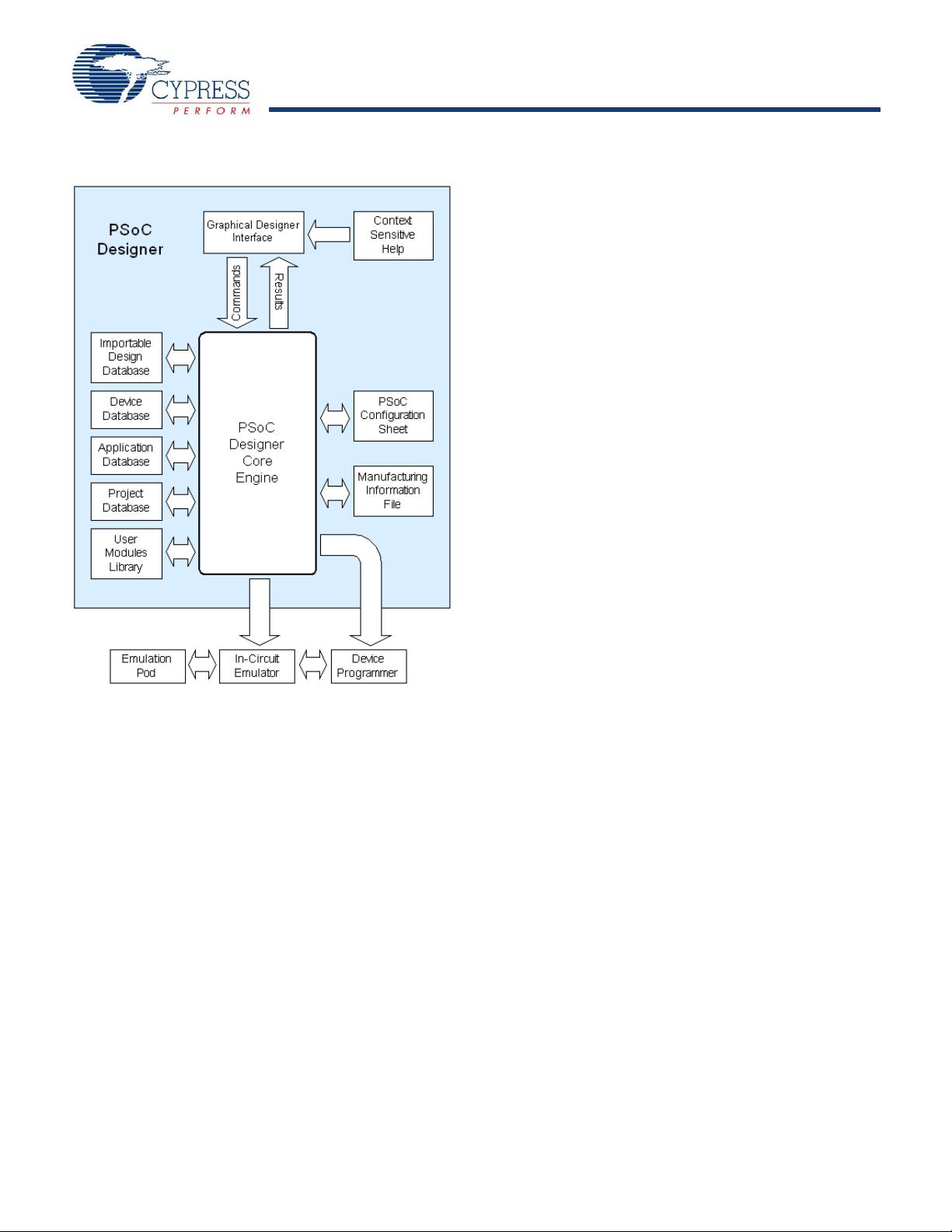
■ Complete Development Tools
❐ Free Development Software
(PSoC Designer™)
❐ Full-Featured, In-Circuit Emulator and Programmer
❐ Full Speed Emulation
❐ Complex Breakpoint Structure
❐ 128K Trace Memory
■ Precision, Programmable Clocking
❐ Internal ±2.5% 24/48 MHz Oscillator
❐ Internal Oscillator for Watchdog and Sleep
■ Programmable Pin Configurations
❐ 25 mA Sink, 10 mA Drive on All GPIO
❐ Pull Up, Pull Down, High Z, Strong, or Open Drain Drive
Modes on All GPIO
❐ Up to 8 Analog Inputs on GPIO
❐ Configurable Interrupt on All GPIO
■ Versatile Analog Mux
❐ Common Internal Analog Bus
❐ Simultaneous Connection of IO Combinations
❐ Capacitive Sensing Application Capability
■ Additional System Resources
❐ I
2
C™ Master, Slave and Multi-Master to 400 kHz
❐ Watchdog and Sleep Timers
❐ User-Configurable Low Voltage Detection
❐ Integrated Supervisory Circuit
❐ On-Chip Precision Voltage Reference
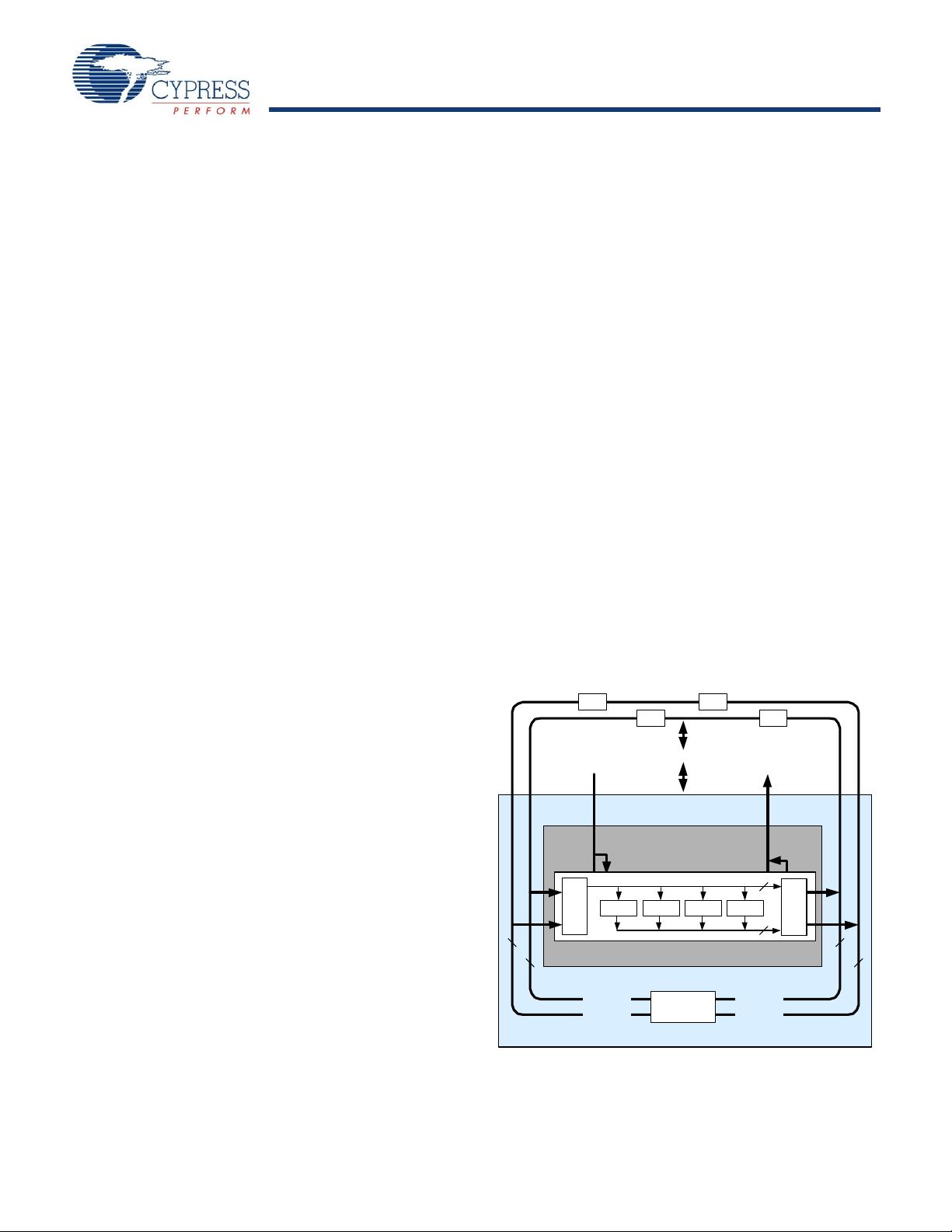
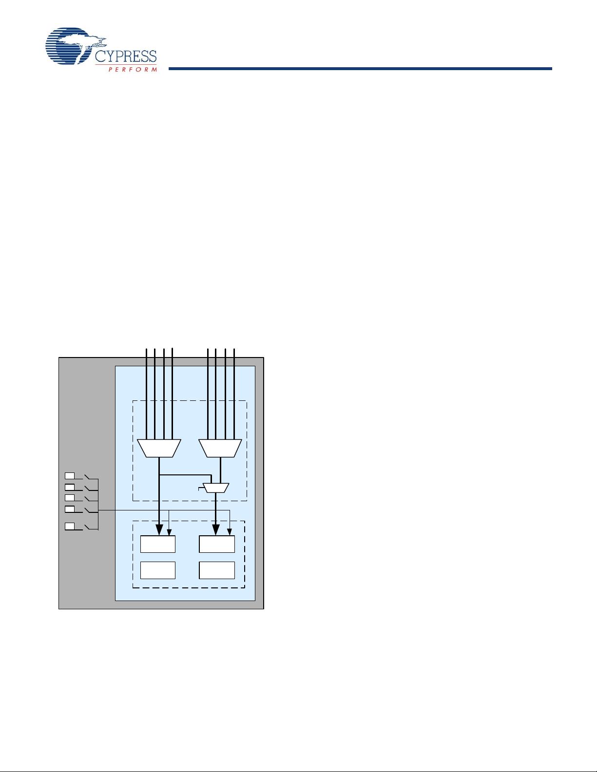
Logic Block Diagram
[+] Feedback
CY8C21634, CY8C21534
CY8C21434, CY8C21334, CY8C21234
Document Number: 38-12025 Rev. *N Page 2 of 45
PSoC Functional Overview
The PSoC family consists of many Mixed-Signal Array with
On-Chip Controller devices. These devices are designed to
replace multiple traditional MCU-based system components with
one low cost single-chip programmable component. A PSoC
device includes configurable blocks of analog and digital logic,
and programmable interconnect. This architecture enables the
user to create customized peripheral configurations, to match
the requirements of each individual application. Additionally, a
fast CPU, Flash program memory, SRAM data memory, and
configurable IO are included in a range of convenient pinouts.
The PSoC architecture, shown in Figure 1, consists of four main
areas: the Core, the System Resources, the Digital System, and
the Analog System. Configurable global bus resources allow
combining all the device resources into a complete custom
system. Each CY8C21x34 PSoC device includes four digital
blocks and four analog blocks. Depending on the PSoC
package, up to 28 general purpose IO (GPIO) are also included.
The GPIO provide access to the global digital and analog inter-
connects.
The PSoC Core
The PSoC Core is a powerful engine that supports a rich
instruction set. It encompasses SRAM for data storage, an
interrupt controller, sleep and watchdog timers, and IMO
(internal main oscillator) and ILO (internal low speed oscillator).
The CPU core, called the M8C, is a powerful processor with
speeds up to 24 MHz. The M8C is a four MIPS 8-bit Harvard
architecture microprocessor.
System Resources provide the following additional capabilities:
■ Digital clocks to increase the flexibility of the PSoC
mixed-signal arrays.
■ I2C functionality to implement an I2C master and slave.
■ An internal voltage reference, MultiMaster, that provides an
absolute value of 1.3V to a number of PSoC subsystems.
■ A switch mode pump (SMP) that generates normal operating
voltages off a single battery cell.
■ Various system resets supported by the M8C.
The Digital System consists of an array of digital PSoC blocks
that may be configured into any number of digital peripherals.
The digital blocks are connected to the GPIO through a series of
global buses that can route any signal to any pin, freeing designs
from the constraints of a fixed peripheral controller.
The Analog System consists of four analog PSoC blocks,
supporting comparators and analog-to-digital conversion up to 8
bits in precision.
The Digital System
The Digital System consists of 4 digital PSoC blocks. Each block
is an 8-bit resource that is used alone or combined with other
blocks to form 8, 16, 24, and 32-bit peripherals, which are called
user module references. Digital peripheral configurations include
the following.
■ PWMs (8 to 32 bit)
■ PWMs with Dead band (8 to 32 bit)
■ Counters (8 to 32 bit)
■ Timers (8 to 32 bit)
■ UART 8 bit with selectable parity
■ SPI master and slave
■ I2C slave and multi-master
■ Cyclical Redundancy Checker/Generator (8 to 32 bit)
■ IrDA
■ Pseudo Random Sequence Generators (8 to 32 bit)
The digital blocks are connected to any GPIO through a series
of global buses that can route any signal to any pin. The buses
also allow for signal multiplexing and for performing logic
operations. This configurability frees your designs from the
constraints of a fixed peripheral controller.
Digital blocks are provided in rows of four, where the number of
blocks varies by PSoC device family. This allows the optimum
choice of system resources for your application. Family
resources are shown in Ta ble 1 on page 4.
Figure 1. Digital System Block Diagram
DIGITAL SYSTEM
To System Bus
D
i
g
i
t
a
l
C
l
o
c
k
s
F
r
o
m
C
o
r
e
Digital PSoC Block Array
To Analog
System
8
Row Input
Configuration
Row Output
Configuration
88
8
Row 0
DBB00 DBB01 DCB02 DCB03
4
4
GIE[7:0]
GIO[7:0]
GOE[7:0]
GOO[7:0]
Global Digital
Interconnect
Por t 3
Por t 2
Por t 1
Por t 0
[+] Feedback
CY8C21634, CY8C21534
CY8C21434, CY8C21334, CY8C21234
Document Number: 38-12025 Rev. *N Page 3 of 45
The Analog System
The Analog System consists of 4 configurable blocks that allow
the creation of complex analog signal flows. Analog peripherals
are very flexible and may be customized to support specific
application requirements. Some of the common PSoC analog
functions for this device (most available as user modules) are:
■ Analog-to-digital converters (single or dual, with 8-bit or 10-bit
resolution)
■ Pin-to-pin comparator
■ Single-ended comparators (up to 2) with absolute (1.3V)
reference or 8-bit DAC reference
■ 1.3V reference (as a System Resource)
In most PSoC devices, analog blocks are provided in columns of
three, which includes one CT (Continuous Time) and two SC
(Switched Capacitor) blocks. The CY8C21x34 devices provide
limited functionality Type “E” analog blocks. Each column
contains one CT Type E block and one SC Type E block. Refer
to the PSoC Programmable System-on-Chip™ Technical
Reference Manual for detailed information on the CY8C21x34’s
Type E analog blocks.
Figure 2. Analog System Block Diagram
The Analog Multiplexer System
The Analog Mux Bus can connect to every GPIO pin. Pins may
be connected to the bus individually or in any combination. The
bus also connects to the analog system for analysis with
comparators and analog-to-digital converters. An additional 8:1
analog input multiplexer provides a second path to bring Port 0
pins to the analog array.
Switch control logic enables selected pins to precharge
continuously under hardware control. This enables capacitive
measurement for applications such as touch sensing. Other
multiplexer applications include:
■ Track pad, finger sensing.
■ Chip-wide mux that allows analog input from any IO pin.
■ Crosspoint connection between any IO pin combinations.
When designing capacitive sensing applications, refer to the
signal-to-noise system level requirement found in Application
Note AN2403 on the Cypress web site at
http://www.cypress.com.
Additional System Resources
System Resources, some of which are listed in the previous
sections, provide additional capability useful to complete
systems. Additional resources include a switch mode pump, low
voltage detection, and power on reset. Brief statements
describing the merits of each system resource follow.
■ Digital clock dividers provide three customizable clock
frequencies for use in applications. The clocks may be routed
to both the digital and analog systems. Additional clocks can
be generated using digital PSoC blocks as clock dividers.
■ The I2C module provides 100 and 400 kHz communication over
two wires. Slave, master, and multi-master modes are all
supported.
■ Low Voltage Detection (LVD) interrupts can signal the
application of falling voltage levels, while the advanced POR
(Power On Reset) circuit eliminates the need for a system
supervisor.
■ An internal 1.3 voltage reference provides an absolute
reference for the analog system, including ADCs and DACs.
■ An integrated switch mode pump (SMP) generates normal
operating voltages from a single 1.2V battery cell, providing a
low cost boost converter.
■ Versatile analog multiplexer system.
AC O L 1 M U X
ACE00 ACE01
Array
Array Input
Configuration
ASE10 ASE11
X
X
X
X
X
An a l o g Mu x Bus
All IO
ACI0[1:0] ACI1[1:0]
[+] Feedback
CY8C21634, CY8C21534
CY8C21434, CY8C21334, CY8C21234
Document Number: 38-12025 Rev. *N Page 4 of 45
PSoC Device Characteristics
Depending on your PSoC device characteristics, the digital and
analog systems can have 16, 8, or 4 digital blocks and 12, 6, or
4 analog blocks. Table 1 lists the resources available for specific
PSoC device groups. The PSoC device covered by this data
sheet is highlighted in this table.
Getting Started
The quickest path to understanding the PSoC silicon is by
reading this data sheet and using the PSoC Designer Integrated
Development Environment (IDE). This data sheet is an overview
of the PSoC integrated circuit and presents specific pin, register,
and electrical specifications. For in-depth information with
detailed programming information, refer the PSoC Program-
mable System-on-Chip Technical Reference Manual available at
http://www.cypress.com/psoc.
For up-to-date Ordering, Packaging, and Electrical Specification
information, refer the latest PSoC device data sheets at
http://www.cypress.com.
Development Kits
Development Kits are available from the following distributors:
Digi-Key, Avnet, Arrow, and Future. The Cypress Online Store
contains development kits, C compilers, and all accessories for
PSoC development. Go to the Cypress Online Store web site at
http://www.cypress.com, click the Online Store shopping cart
icon at the bottom of the web page, and click PSoC (Program-
mable System-on-Chip) to view a current list of available items.
Technical Training Modules
Free PSoC technical training modules are available for users
new to PSoC. Training modules cover designing, debugging,
advanced analog and CapSense. Go to
http://www.cypress.com/techtrain.
Consultants
Certified PSoC Consultants offer everything from technical
assistance to completed PSoC designs. To contact or become a
PSoC Consultant go to http://www.cypress.com, click on Design
Support located on the left side of the web page, and select
CYPros Consultants.
Technical Support
PSoC application engineers take pride in fast and accurate
response. They can be reached with a 4-hour guaranteed
response at http://www.cypress.com/support.
Application Notes
A long list of application notes can assist you in every aspect of
your design effort. To view the PSoC application notes, go to the
http://www.cypress.com web site and select Application Notes
under the Design Resources list located in the center of the web
page. Application notes are sorted by date by default.
Development Tools
PSoC Designer is a Microsoft
®
Windows-based, integrated
development environment for the Programmable
System-on-Chip (PSoC) devices. The PSoC Designer IDE and
application runs on Windows NT 4.0, Windows 2000, Windows
Millennium (Me), or Windows XP. (See Figure 3 on page 5)
PSoC Designer helps the customer to select an operating
configuration for the PSoC, write application code that uses the
PSoC, and debug the application. This system provides design
database management by project, an integrated debugger with
In-Circuit Emulator, in-system programming support, and the
CYASM macro assembler for the CPUs.
PSoC Designer also supports a high-level C language compiler
developed specifically for the devices in the family.
Table 1. PSoC Device Characteristics
PSoC Part
Number
Digital
IO
Digital
Rows
Digital
Blocks
Analog
Inputs
Analog
Outputs
Analog
Columns
Analog
Blocks
SRAM
Size
Flash
Size
CY8C29x66 up to
64
4 16 12 4 4 12 2K 32K
CY8C27x43
up to
44
2 8 12 4 4 12 256
Bytes
16K
CY8C24x94 56 1 4 48 2 2 6 1K 16K
CY8C24x23A
up to
24
1 4 12 2 2 6 256
Bytes
4K
CY8C21x34 up to
28
1 4 28 0 2 4
[1]
512
Bytes
8K
CY8C21x23
16 1 4 8 0 2 4
[1]
256
Bytes
4K
CY8C20x34
up to
28
0 0 28 0 0 3
[2]
512
Bytes
8K
Notes
1. Limited analog functionality
.
2. Two analog blocks and one CapSense.
[+] Feedback
CY8C21634, CY8C21534
CY8C21434, CY8C21334, CY8C21234
Document Number: 38-12025 Rev. *N Page 5 of 45
Figure 3. PSoC Designer Subsystems
PSoC Designer Software Subsystems
Device Editor
The device editor subsystem enables the user to select different
onboard analog and digital components called user modules
using the PSoC blocks. Examples of user modules are ADCs,
DACs, Amplifiers, and Filters.
The device editor also supports easy development of multiple
configurations and dynamic reconfiguration. Dynamic
reconfiguration allows changing configurations at run time.
PSoC Designer sets up power on initialization tables for selected
PSoC block configurations and creates source code for an
application framework. The framework contains software to
operate the selected components and, if the project uses more
than one operating configuration, contains routines to switch
between different sets of PSoC block configurations at run time.
PSoC Designer can print out a configuration sheet for a given
project configuration for use during application programming in
conjunction with the Device Data Sheet. After the framework is
generated, the user can add application-specific code to flesh
out the framework. It is also possible to change the selected
components and regenerate the framework.
Design Browser
The Design Browser enables users to select and import
preconfigured designs into the user’s project. Users can easily
browse a catalog of preconfigured designs to facilitate
time-to-design. Examples provided in the tools include a
300-baud modem, LIN Bus master and slave, fan controller, and
magnetic card reader.
Application Editor
In the Application Editor you can edit your C language and
Assembly language source code. You can also assemble,
compile, link, and build.
Assembler. The macro assembler allows the seamless
merging of the assembly code with C code. The link libraries
automatically use absolute addressing or are compiled in relative
mode, and linked with other software modules to get absolute
addressing.
C Language Compiler. A C language compiler that supports
the PSoC family of devices is available. Even if you have never
worked in the C language before, the product quickly helps you
create complete C programs for the PSoC family devices.
The embedded, optimizing C compiler provides all the features
of C tailored to the PSoC architecture. It comes complete with
embedded libraries providing port and bus operations, standard
keypad and display support, and extended math functionality.
Debugger
The PSoC Designer Debugger subsystem provides hardware
in-circuit emulation, allowing the designer to test the program in
a physical system while providing an internal view of the PSoC
device. Debugger commands allow the designer to read the
program and read and write data memory, read and write IO
registers, read and write CPU registers, set and clear break-
points, and provide program run, halt, and step control. The
debugger also allows the designer to create a trace buffer of
registers and memory locations of interest.
Online Help System
The online help system displays online, context-sensitive help
for the user. Designed for procedural and quick reference, each
functional subsystem has its own context-sensitive help. This
system also provides tutorials and links to FAQs and an Online
Support Forum to aid the designer in getting started.
Hardware Tools
In-Circuit Emulator
A low cost, high functionality ICE (In-Circuit Emulator) is
available for development support. This hardware has the
capability to program single devices.
The emulator consists of a base unit that connects to the PC by
way of a USB port. The base unit is universal and operates with
all PSoC devices. Emulation pods for each device family are
available separately. The emulation pod takes the place of the
PSoC device in the target board and performs full speed
(24 MHz) operation.
[+] Feedback
剩余44页未读,继续阅读
ls136112
- 粉丝: 0
- 资源: 1
上传资源 快速赚钱
- 我的内容管理 收起
- 我的资源 快来上传第一个资源
- 我的收益 登录查看自己的收益
- 我的积分 登录查看自己的积分
- 我的C币 登录后查看C币余额
- 我的收藏
- 我的下载
- 下载帮助
会员权益专享
最新资源
- RTL8188FU-Linux-v5.7.4.2-36687.20200602.tar(20765).gz
- c++校园超市商品信息管理系统课程设计说明书(含源代码) (2).pdf
- 建筑供配电系统相关课件.pptx
- 企业管理规章制度及管理模式.doc
- vb打开摄像头.doc
- 云计算-可信计算中认证协议改进方案.pdf
- [详细完整版]单片机编程4.ppt
- c语言常用算法.pdf
- c++经典程序代码大全.pdf
- 单片机数字时钟资料.doc
- 11项目管理前沿1.0.pptx
- 基于ssm的“魅力”繁峙宣传网站的设计与实现论文.doc
- 智慧交通综合解决方案.pptx
- 建筑防潮设计-PowerPointPresentati.pptx
- SPC统计过程控制程序.pptx
- SPC统计方法基础知识.pptx
资源上传下载、课程学习等过程中有任何疑问或建议,欢迎提出宝贵意见哦~我们会及时处理!
点击此处反馈
安全验证
文档复制为VIP权益,开通VIP直接复制
信息提交成功
评论2