没有合适的资源?快使用搜索试试~ 我知道了~
首页开关电源PCB布线技术
开关电源PCB布线技术
4星 · 超过85%的资源 需积分: 16 18 下载量 67 浏览量
更新于2023-03-03
评论
收藏 229KB PDF 举报
开关电源PCB布线技术 美国模拟器件公司工程师写的文章,对于设计开关电源PCB有很大的帮助
资源详情
资源评论
资源推荐
SIMPLE SWITCHER
®
PCB
Layout Guidelines
Introduction
One problem with writing an Application Note on PCB layout
is that the people who read it are usually not the ones who
are going to use it. Even if the designer has struggled
through electromagnetic fields, EMC, EMI, board parasitics,
transmission line effects, grounding, etc., he will in all prob-
ability then go on with his primary design task, leaving the
layout to the CAD/layout person. Unfortunately, especially
when it comes to switching regulators, it is not enough to be
concerned with just basic routing/connectivity and mechani-
cal issues. Both the designer and the CAD person need
to be aware that the design of a switching power con-
verter is only as good as its layout. Which probably ex-
plains why a great many of customer calls received, con-
cerning switcher applications, are ultimately traced to poor
layout practices. Sadly, these could and should have been
avoided on the very first prototype board, saving time and
money on all sides.
The overall subject of PCB design is an extremely wide one,
embracing several test/mechanical/production issues and
also in some cases compliance/regulatory issues. There is
also a certain amount of physics/electromagnetics involved,
if a clearer understanding is sought. But the purpose of this
Application Note is to reach the audience most likely to use
it. Though there is enough design information for the more
experienced designer/CAD person, the Application Note in-
cludes a quick-set of clear and concise basic rules that
should be scrupulously followed to avoid a majority of prob-
lems. In particular, we have provided recommended start-
ing points for layout when using the popular LM267x,
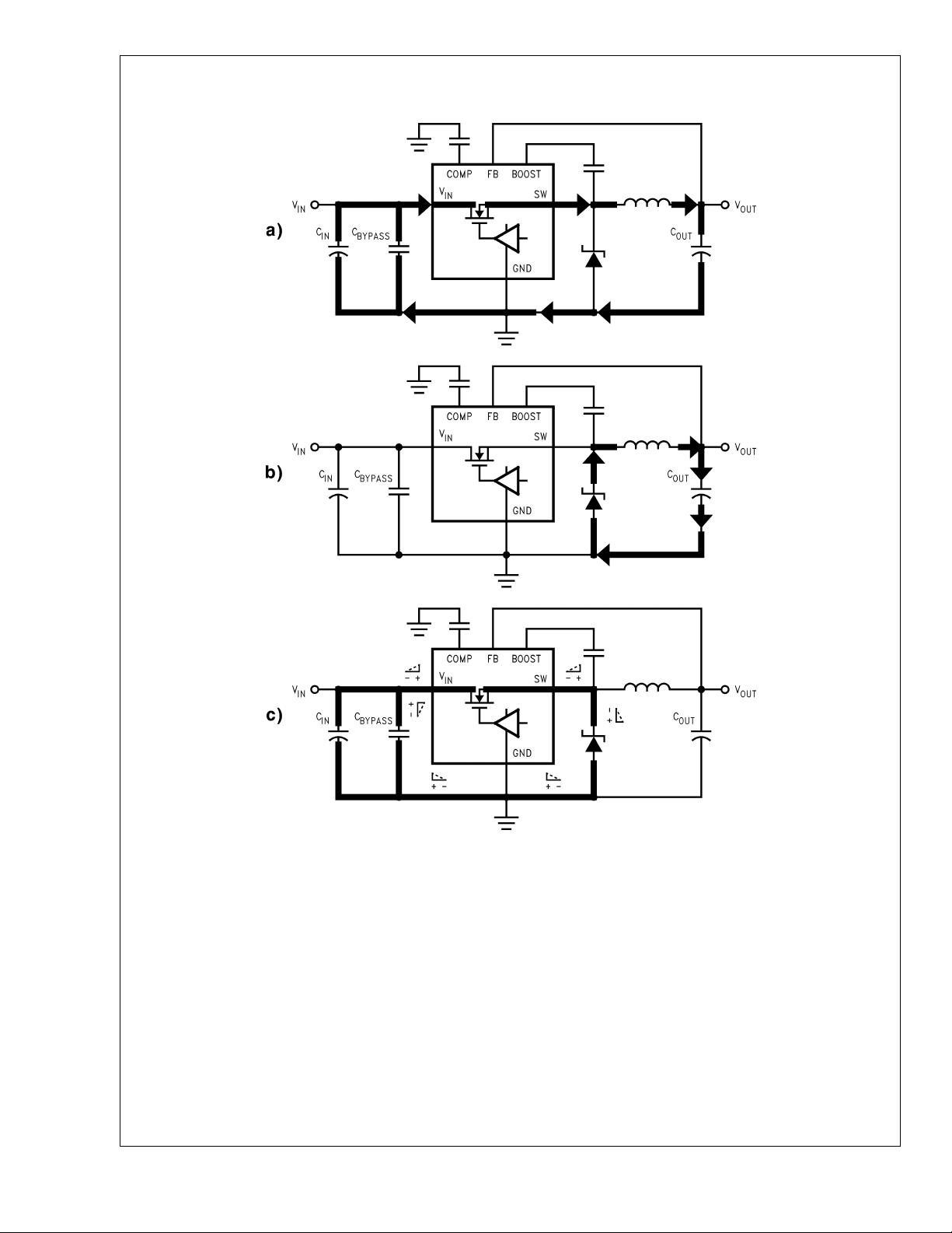
LM259x and LM257x families (Figure 2) The focus is on
the step-down (Buck) Simple Switcher ICs from National, but
the same principles hold for any topology and switching
power application.
Most of the issues discussed in this Note revolve around
simply assuring the desired performance in terms of basic
electrical functionality. Though luckily, as the beleaguered
switcher designer will be happy to know, in general all the
electrical aspects involved are related and point in the same
general ‘direction’. So for example, an ‘ideal’ layout, i.e. one
which helps the IC function properly, also leads to reduced
electromagnetic emissions, and vice-versa. For example,
reducing the area of loops with switching currents will help in
terms of EMI and performance. However the designer is
cautioned that there are some exceptions to this general
’trend’. One which is brought out in some detail here is the
practice of ’copper-filling’, which may help reduce parasitic
inductances and reduce noise-induced IC problems, but can
also increase EMI.
Quick-Set of Rules for SIMPLE SWITCHER PCB Layout (Buck)
a) Place the catch diode and input capacitor as shown in Figure 2.
b) For high-speed devices (e.g. LM267x) do not omit placing input decoupling/bypass ceramic capacitor (0.1
µF–0.47 µF) as in Figure 2.
c) Connect vias to a Ground plane if available (optional, marked ‘X’ in Figure 2)
d) If vias fall under tab of SMT power device, these are considered ‘thermal vias’. Use correct dimensions as
discussed to avoid production issues. Or place the vias close to but not directly under the tab.
e) Route feedback trace correctly as discussed, away from noise sources such as the inductor and the diode.
f) Do not increase width of copper on switching node injudiciously.
g) If very large heatsink area is required for catch diode (having estimated the heatsink requirement correctly) use
isolation as discussed.
h) For higher power SMT applications, use 2 oz board for better thermal management with less copper area.
SIMPLE SWITCHER is a Registered Trademark of National Semiconductor.
National Semiconductor
Application Note 1229
Sanjaya Maniktala
July 2002
SIMPLE SWITCHER PCB Layout Guidelines AN-1229
© 2002 National Semiconductor Corporation AN200426 www.national.com
Introduction (Continued)
The AC and DC Current Paths
Referring to Figure 1a, the bold lines represents the main
(power) current flow in the converter during the time the
switch is ON. As the switch turns ON, the edge of the of the
current waveform is provided largely by CBYPASS, the re-
mainder coming mainly from CIN. Some slower current com-
ponents come from the input DC power supply (not shown)
and also refresh these input caps. Figure 1b represents the
situation when the switch is OFF. We can therefore see that
in certain trace sections, current has to start flowing sud-
denly during the instant of switch turn-off and in some sec-
tions it needs to stop flowing equally suddenly. Figure 1c
represents the ‘difference’, i.e. traces shown bold in this
Figure are those where the current flow changes suddenly.
During the turn-on transition the picture reverses, but the
’difference’ trace sections are the same. Therefore during
either switch transition, ’step changes’ of current take place
in these difference sections. These traces encounter the
harmonic-rich rising or trailing edges of the current pedestal
waveform. The difference traces are considered ’critical’ and
deserve utmost attention during PCB layout. It is often stated
colloquially, that ‘AC current’ flows in these trace sections,
and ’DC current’ in the others. The reason is that the basic
switching PWM frequency forms only a fraction of the total
harmonic (Fourier) content of the current waveform in the
’AC’ traces. In comparison, where ‘DC current’ flows, the
current does not change in a stepped fashion and so the
harmonic content is lower. It is also no surprise that the DC
20042601
FIGURE 1.
AN-1229
www.national.com 2
The AC and DC Current Paths
(Continued)
sections are those in series with the main inductor, because
it is known that inductors have the property of preventing
sudden changes in current (this is analogous to a capacitor
which ‘resists’ sudden changes in voltage).
Summing up: In switching regulator layout, it is the AC
paths that are considered critical, whereas the DC paths
are not. That is the only basic rule to be kept in mind,
and from which all the others follow. This is also true for
any topology. Perform an analysis of the current flow for
any topology in the same manner as we did for the Buck, to
find the ’difference traces’: and these traces are by defintion
the ’critical’ ones for layout.
What is the problem with step current changes anyway? In a
resistor for example, this causes no unexpected/
unidentifiable problem. The voltage is given by V=IR, and so
for a given change of current, the voltage will change pro-
portionally. For example, a 0.5 cm wide Cu trace of thick-
ness 1.4 mil has a resistance of 1milliohm per cm length
(at 20 degC). So it seems that a 1 inch long trace with a
current changeover of 1A, would produce a change in volt-
age of only 2.5 millivolts across the trace, which is insignifi-
cant enough to cause the control sections of most ICs to
misbehave. But in fact the induced voltage is much larger.
The important thing to realize is that traces of copper on a
PCB, though barely resistive, are also inductive. Now, the
oft-repeated thumb-rule is that ‘every inch of trace length
has an inductance of about 20 nH’. Like the trace resis-
tance, that too doesn’t seem much at first sight. But it is this
rather minute inductance which is in fact responsible for a
great many customer calls in SIMPLE SWITCHER applica-
tions!
The equation for voltage across an inductance is V=L
*
dl/dt,
and so the voltage does not depend on the current but on the
rate of change of the current. This fact makes all the differ-
ence when the 1A change we spoke about occurs within a
very short time. The induced voltage can be very high, even
for small inductances and currents, if the dl/dt is high. A high
dl/dt event occurs during transition from Figure 1a to Figure
1b (and back) in all the AC trace sections (shown bold in
Figure 1c). The induced voltage spike appears across each
affected trace, lasting for the duration of the crossover.
To get a better feel for the numbers here: the change in
current in the AC sections of a typical buck converter is
about 1.2 times the load current during the switch
turn-off transition and is about 0.8 times the load current
during the switch turn-on transition (for an ’optimally’
designed Buck inductor, as per inductor design guidelines in
the relevant Datasheets/Selection Software). The transition
time is about 30 ns for high speed Fet switchers like the
LM267x, and is about 75 ns for the slower bipolar switchers
like the LM259x series. This also incidentally means that the
voltage spikes in the high-speed families can be more than
twice that in the slower families, for a comparable layout and
load. Therefore layout becomes all the more critical in
high-speed switchers.
So, one inch of trace switching say 1A of instantaneous
current in a transition time of 30 ns gives 0.7V, as compared
to 2.5mV (that we estimated on the basis of resistance
alone). For 3A, and two inches of trace, the induced voltage
’tries’ to be 4V! In Figure 1c, the small triangles along the
sections indicate the direction of the momentary induced
voltage, as the converter changes from the situation in Fig-
ure 1a to that in Figure 1b (switch turn-off). We can see that
assuming that the ground pin of the IC is the reference point,
the switching node (marked ‘SW’) tries to go negative (all its
series trace sections adding up). Similarly the input pin
(marked ‘VIN’ goes high through series contributions in all its
related sections. Figure 1c represents the picture during the
turn-off transition. During the turn-on transition all the in-
duced voltage polarities shown are simply reversed. In that
case, the VIN pin is dragged low, and the switching node pin
is dragged high momentarily.
The astute designer will recognize that this was to be ex-
pected since any inductance, even if it is parasitic, demands
to be ‘reset’, which means that the volt-seconds during the
on-time must equal and be opposite in sign to the
volt-seconds during the off-time.The designer will also real-
ize that till these parasitic trace inductances reset, they do
not ’allow’ the crossover to occur. So for example, traces
which were carrying current prior to switch turn-off will ’insist’
on carrying current till the voltage spikes force them to do
otherwise. Similarly, the traces which need to start carrying
current will ’refuse’ to do so till the spikes across them force
them to do likewise. Since switching losses are proportional
to crossover time, even if these voltage spikes do not cause
anomalous behavior, they can degrade efficiency. For ex-
ample, in transformer-based flyback regulators, when the the
primary number of turns is much larger than the secondary
turns, designers may be surprised to learn how much the
secondary side trace inductances alone can degrade effi-
ciency. This is because any secondary side uncoupled
(trace/transformer leakage) inductances reflect into the
primary side as an equivalent parasitic inductance in
series with the switch. This adds an additional term to
the effective leakage as seen by the switch that equals
the secondary inductance multiplied by square of the
turns ratio (turns ratio being Np/Ns). Therefore the dissipa-
tion in the flyback clamp (zener/RCD) can increase dramati-
cally, lowering efficiency. One lesson here is that though
’leakage inductance’ (from traces or the transformer) is con-
sidered ’uncoupled’, in reality it can make its presence se-
verely felt from one side of the transformer to the other. So it
is not totally ’uncoupled’ at all! In fact this happens to be the
main reason why flybacks with low output voltages (high
turns ratio) show poorer efficiency as compared to higher
output flybacks. Therefore, reducing critical trace induc-
tances is important for several reasons: efficiency, EMI, be-
sides basic functionality.
The momentary voltage spikes which last for the duration of
the transition can be very hard to capture on an oscilloscope.
But they may be presumed to be present if the IC is seen to
be misbehaving for no ’obvious reason’. These spikes, if
present with sufficiently high amplitude, can propagate into
the control sections of the IC causing what we call here a
controller ’upset’. This leads to the observed performance
anomalies, and in rare cases this can even cause device
failure. Since none of these spike-related problems can be
easily corrected, or band-aided, once the layout is initially
bad, the important thing is to get the layout ‘right’ to start
with.
The designer may well ask, why is it that these step current
changes are a problem with the parasitic trace inductances,
and not with the main inductor of the Buck converter? That is
because all inductors try to resist any sudden current
change. But since the main inductor has a much larger
inductance (and energy storage) as compared to the para-
sitic trace inductances, it therefore ends up ‘dominating’.
From V
*
dt=L
*
dl we can also see that if L is large, a much
higher voltseconds (V
*
dt) is required to cause a given
AN-1229
www.national.com3
剩余11页未读,继续阅读
lpc2132
- 粉丝: 0
- 资源: 8
上传资源 快速赚钱
- 我的内容管理 收起
- 我的资源 快来上传第一个资源
- 我的收益 登录查看自己的收益
- 我的积分 登录查看自己的积分
- 我的C币 登录后查看C币余额
- 我的收藏
- 我的下载
- 下载帮助
会员权益专享
最新资源
- 27页智慧街道信息化建设综合解决方案.pptx
- 计算机二级Ms-Office选择题汇总.doc
- 单链表的插入和删除实验报告 (2).docx
- 单链表的插入和删除实验报告.pdf
- 物联网智能终端项目设备管理方案.pdf
- 如何打造品牌的模式.doc
- 样式控制与页面布局.pdf
- 武汉理工Java实验报告(二).docx
- 2021线上新品消费趋势报告.pdf
- 第3章 Matlab中的矩阵及其运算.docx
- 基于Web的人力资源管理系统的必要性和可行性.doc
- 基于一阶倒立摆的matlab仿真实验.doc
- 速运公司物流管理模式研究教材
- 大数据与管理.pptx
- 单片机课程设计之步进电机.doc
- 大数据与数据挖掘.pptx
资源上传下载、课程学习等过程中有任何疑问或建议,欢迎提出宝贵意见哦~我们会及时处理!
点击此处反馈
安全验证
文档复制为VIP权益,开通VIP直接复制
信息提交成功
评论1