没有合适的资源?快使用搜索试试~ 我知道了~
首页cypress usb开发教程
cypress usb开发教程
5星 · 超过95%的资源 需积分: 50 36 下载量 40 浏览量
更新于2023-03-03
评论
收藏 130KB PDF 举报
Cypress鼠标开发教程,英文原版,Cypress鼠标开发教程,英文原版。
资源详情
资源评论
资源推荐
fax id: 3450
Cypress Semiconductor Corporation
• 3901 North First Street • San Jose • CA 95134 • 408-943-2600
Januar
y
21
,
1997 - Revised October 30
,
1997
Designing a Low-Cost USB Mouse with the Cypress
Semiconductor CY7C63000 USB Controller
Introduction
The Universal Serial Bus (USB) is an industrial standard se-
rial interface between a computer and peripherals such as a
mouse, joystick, keyboard, etc. This application note de-
scribes how a cost-effective USB opto-mechanical mouse
can be built quickly using the Cypress Semiconductor sin-
gle-chip CY7C63000 USB controller. The document starts
with the basic operations of an opto-mechanical mouse fol-
lowed by an introduction to the CY7C63000 USB controller.
A schematic of the USB mouse and its connection details can
be found in the Hardware Implementation Section.
The software section of this application note describes the
architecture of the firmware required to implement the mouse
function. Several sample code segments are included to as-
sist in the explanation. The binary code of the complete
mouse firmware is available free of charge from Cypress
Semiconductor. Please contact your local Cypress sales of-
fice for details.
This application note assumes that the reader is familiar with
the CY7C63000 USB controller and the Universal Serial Bus.
The CY7C63000 data sheet is available from the Cypress
web site at www.cypress.com. USB documentation can be
found at the USB Implementers Forum web site at
www.usb.org.
USB Mouse Basics
USB has been gaining popularity due to it’s simple connec-
tion, plug and play feature, and hot insertion capability. There
are several kinds of USB pointing devices available in the
market. The opto-mechanical mouse is the most popular type
because it provides relatively high resolution and works on a
wide range of surfaces.
Basically, an opto-mechanical mouse has a rubber track ball
that is coupled to two roll bars as shown in
Figure 1
. The
“stabilizer” is a roller that provides the third contact point for
the mouse ball.
One roll bar keeps track of the X-axis movement while the
other one keeps track of the Y-axis movement. There is a
slotted wheel at one end of each roll bar. An LED is installed
on one side of the wheel with two photo transistors positioned
on the other side as shown in
Figure 2
.
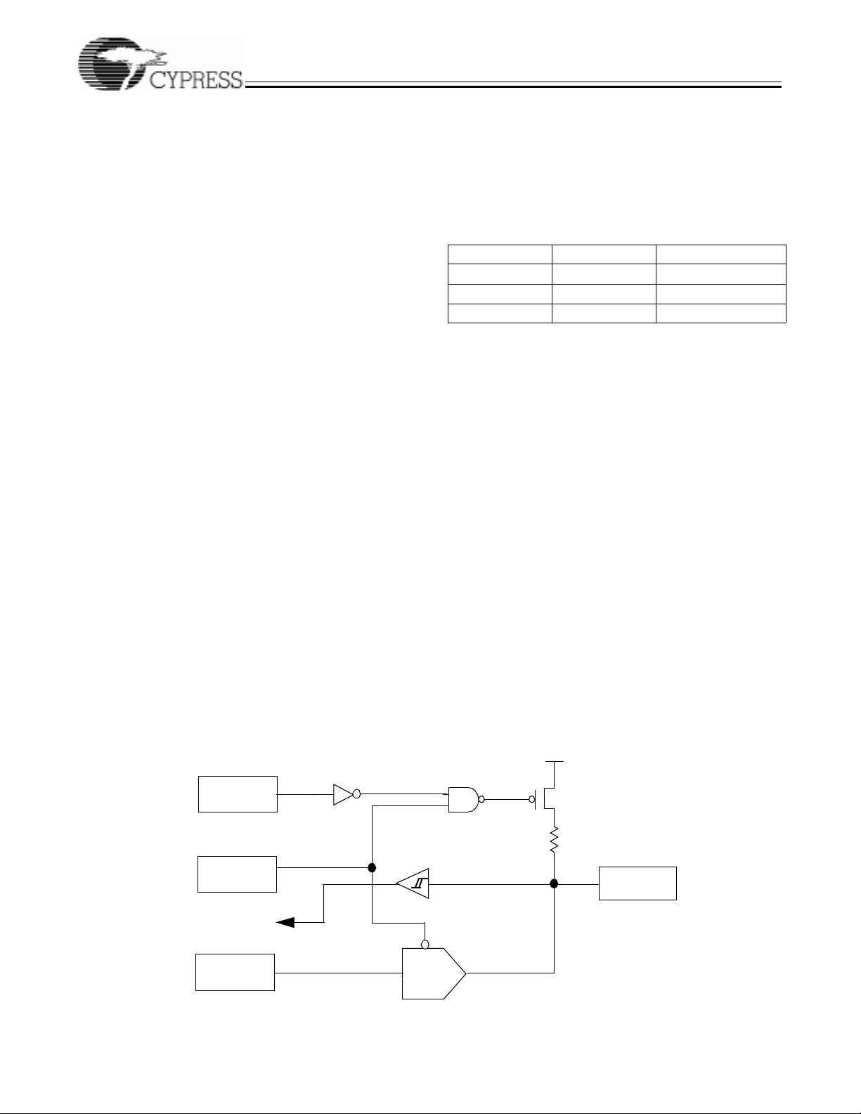
The photo-transistor outputs allow the mouse to detect wheel
motion and determine the motion direction. For example, from
the starting position shown, wheel motion to the left would
look like
Figure 3
.
From the starting position shown, slotted wheel motion to the
right would look like
Figure 4
.
From the outputs of the photo-transistors, the mouse chip de-
termines the direction and calculates the distance when the
mouse is moved.
Figure 1. Mechanical Hardware
Figure 2. Opto-Mechanical Detail
Figure 3. Slotted Wheel Moves Left
Figure 4. Slotted Wheel Moves Right
mouse ball
X-axis roller
Y-axis roller
slotted wheel
stabilizer
slotted wheel
LED
photo transistors
LED
slotted
wheel
two photo
transistors
PT1 PT2
PT1
PT2
on
off
PT1
PT2
on
off
Designing a Low-Cost USB Mouse
2
The resolution is the smallest motion the mouse can detect,
measured in dots per inch (DPI). A typical opto-mechanical
mouse has a resolution in the 200 to 400 DPI range. The
mechanical dimensions of the mouse hardware limit the max-
imum achievable resolution.
USB provides the plug-and-play feature that is not supported
in RS-232 and PS/2 interfaces. The USB interface uses a
four-pin connector with positive retention. A 28 AWG twisted
pair is used for differential signaling and two 20 to 30 AWG
wires are used to supply power and ground. No cable shield-
ing is necessary for a mouse application.
Introduction to CY7C63000
The CY7C63000 is a high performance 8-bit RISC microcon-
troller with an integrated USB Serial Interface Engine (SIE).
The architecture implements 34 commands that are opti-
mized for USB applications. The CY7C63000 has built-in
clock oscillator and timers as well as programmable current
drivers, and pull-up resistors at each I/O line. High perfor-
mance, low-cost human-interface type computer peripherals
such as mouse, joystick, and gamepad can be implemented
with minimum external components and firmware effort.
Clock Circuit
The CY7C63000 has a built-in clock oscillator and PLL-based
frequency doubler. This circuit allows a cost effective 6 MHz
ceramic resonator to be used externally while the on-chip
RISC core runs at 12 MHz.
USB Serial Interface Engine (SIE)
The operation of the SIE is totally transparent to the user. In
the receive mode, USB packet decode and data transfer to
the endpoint FIFO are automatically done by the SIE. The SIE
then generates an interrupt request to invoke the service rou-
tine after a packet is unpacked.
In the transmit mode, data transfer from the endpoint and the
assembly of the USB packet are handled automatically by the
SIE.
General Purpose I/O
The CY7C63000 has 12 general purpose I/O lines divided
into 2 ports: Port 0 and Port 1. One such I/O circuit is shown
in
Figure 5
. The output state can be programmed according
to
Table 1
below
.
Writing a “0” to the Data Register will drive
the output Low and allow it to sink current.
Instead of supporting a fixed output drive, the CY7C63000
allows the user to select an output current level for each I/O
line. The sink current of each output is controlled by a dedi-
cated 8-bit Isink Register. The lower 4-bits of this register con-
tains a code selecting one of sixteen sink current levels. The
upper 4-bits are reserved and must be written as zeros. The
output sink current levels of the two I/O ports are different. For
Port 0 outputs, the lowest drive strength (0000) is about 0.2
mA and the highest drive strength (1111) is about 1.0 mA.
These levels are insufficient to drive the LEDs in a mouse.
Port 1 outputs are specially designed to drive high-current
applications such as LEDs. Each Port 1 output is much stron-
ger than their Port 0 counterparts at the same drive level set-
ting. In other words, the lowest and highest drive for Port 1
lines are 3.2 mA and 16 mA respectively.
Each General Purpose I/O (GPIO) is capable of generating
an interrupt to the RISC core. Interrupt polarity is selectable
on a per bit basis using the Port Pull-up register. Setting a Port
Pull-up register bit to “1” will select a rising edge trigger for the
corresponding GPIO line. Conversely, setting a Port Pull-up
Register bit to “0” will select a falling edge trigger. The inter-
rupt triggered by a GPIO line is individually enabled by a ded-
icated bit in the Port Interrupt Enable Registers. All GPIO in-
terrupts are further masked by the Global GPIO Interrupt
Enable Bit in the Global Interrupt Enable Register.
Table 1. Programmable Output State
Port Data bit Port Pull-up bit Output State
0 X sink current “0”
1 0 pull-up resistor “1”
1 1 High-Z
Figure 5. One General Purpose I/O Line
GPIO
Pin
V
CC
Isink
DAC
Port Isink
Register
Port Data
Register
Port Pull-Up
Register
16 K
Ω
Schmitt
Trigger
Data Bus
Designing a Low-Cost USB Mouse
3
The Port Pull-up Registers are located at I/O address 0x08
and 0x09 for Port 0 and Port 1 respectively. The Data Regis-
ters are located at I/O address 0x00 and 0x01 for Port 0 and
Port 1 respectively. The Port 0 and Port 1 Interrupt Enable
Registers are at addresses 0x04 and 0x05 respectively.
Wake-Up Interrupt
Power management is paramount in many USB applications.
To conserve power, the CY7C63000 supports an externally
programmable interrupt input to wake up the microcontroller
from the suspend mode when the mouse is moved or when a
button is pressed. The suspend mode causes the microcon-
troller to shut down most of its functions such as the clock
circuit, the RISC core, the timer, and part of the SIE. In the
mouse application, a high percentage of the power is con-
sumed by the LEDs. Therefore, the CY7C63000 should be
programmed to turn off the LEDs before entering the suspend
mode. With the LEDs off, the CY7C63000 can no longer de-
tect any mouse movements although button closures are still
recognized (because pressing a button causes an interrupt).
This problem can be solved by using the wake-up interrupt
that wakes up the microcontroller, checks for mouse move-
ment, and then goes back to suspend mode.
The wake-up interrupt can be implemented by connecting the
CEXT pin to VCC with a resistor and to GND with a capacitor.
Before the firmware puts the microcontroller into the suspend
mode, it writes a zero to the Cext register at address 0x22 to
discharge the external capacitor. Then, to start timing a one
is written to the Cext register to allow the RC circuit to begin
charging. A wake-up interrupt is generated to the RISC core
when the external capacitor is charged up to nominal 2.75V
(45% to 65% of Vcc) by the external resistor. The duration
between successive wake-ups is controlled by the RC con-
stant of the external resistor and capacitor.
Hardware Implementation
Figure 6
is the schematic for a mouse application.
Photo transistor pins of Port 0 are programmed by writing a
zero to the Data Registers which drives the output low. Then
set the value of the Port Isink Register to the sink current
value. One of sixteen sink current values could be selected.
This is done to bias the photo transistors for correct operation.
Button pins of Port 0 are programmed to accept active-low
inputs with internal pull-up resistors enabled. This is accom-
plished by setting all bits in the Port 0 Data Register to “1” and
setting the contents of the Port 0 Pull-up Register to all “0”s.
Bits 4 to 6 of Port 0 are connected to the left, right, and middle
buttons respectively. Bits 0 and 1 are connected to the left and
right photo transistors of the horizontal axis respectively. Bits
2 and 3 are connected to left and right photo transistors of the
vertical axis respectively.
The two LEDs are connected in series to bit 0 of Port 1. The
LEDs are turned off in the suspend mode to conserve power.
The LEDs are switched on only when the mouse wakes up.
Because the sink current of each GPIO line can be set to one
of sixteen levels, the user can adjust the light output of the
LEDs to match the sensitivity of a wide range of photo tran-
sistors.
The CEXT pin of the CY7C63000 is connected to an external
RC timing circuit formed by R2 and C1. The wake-up time is
set to about 20 msec to achieve a good balance between
wake-up response time and power savings.
A 6 MHz ceramic resonator is connected to the clock inputs
of the microcontroller. This component should be placed as
close to the microcontroller as possible.
According to the USB specification, the USB D– line of a
low-speed device (1.5 Mbps) should be tied to a voltage
source between 3.0V and 3.6V with a 1.5K ohms pull-up ter-
minator. The CY7C63000 eliminates the need for a 3.3V reg-
ulator by specifying a 7.5 Kohm resistor connected between
the USB D– line and the nominal 5V Vcc.
剩余10页未读,继续阅读
hecuan1123
- 粉丝: 0
- 资源: 2
上传资源 快速赚钱
- 我的内容管理 收起
- 我的资源 快来上传第一个资源
- 我的收益 登录查看自己的收益
- 我的积分 登录查看自己的积分
- 我的C币 登录后查看C币余额
- 我的收藏
- 我的下载
- 下载帮助
会员权益专享
最新资源
- c++校园超市商品信息管理系统课程设计说明书(含源代码) (2).pdf
- 建筑供配电系统相关课件.pptx
- 企业管理规章制度及管理模式.doc
- vb打开摄像头.doc
- 云计算-可信计算中认证协议改进方案.pdf
- [详细完整版]单片机编程4.ppt
- c语言常用算法.pdf
- c++经典程序代码大全.pdf
- 单片机数字时钟资料.doc
- 11项目管理前沿1.0.pptx
- 基于ssm的“魅力”繁峙宣传网站的设计与实现论文.doc
- 智慧交通综合解决方案.pptx
- 建筑防潮设计-PowerPointPresentati.pptx
- SPC统计过程控制程序.pptx
- SPC统计方法基础知识.pptx
- MW全能培训汽轮机调节保安系统PPT教学课件.pptx
资源上传下载、课程学习等过程中有任何疑问或建议,欢迎提出宝贵意见哦~我们会及时处理!
点击此处反馈
安全验证
文档复制为VIP权益,开通VIP直接复制
信息提交成功
评论1