
Design steps taken from
1) www.ece.utah.edu/~harrison/ece5720/opampsim1.pdf
2) www.ece.utah.edu/~harrison/ece5720/opampsim2.pdf
This assignment will take you through the simulation and basic characterization of a simple
operational amplifier (opamp).
While most digital circuits use a single-polarity power supply (e.g., vdd and gnd), many
analog circuits . especially op amps are powered by a dual-polarity power supply (e.g., vdd,
vss, and gnd). By convention, vdd is positive relative to gnd (e.g.,+1.2V) and vss is negative
relative to gnd (e.g., -1.2V). The use of dual-polarity power supplies allows us to center ac
signals at gnd and build circuits capable of generating signals that swing above and below
gnd by a few volts.
However the current technology offers only single polarity supply where the vdd=1.2V and
the negative supply is gnd=0V. In order to design the opamp we need to redefine the single
polarity supply using the analog ground gnda.
This voltage can be given by the component gnda from the analogLib library in cadence
gnda=600m. So now we have something similar to a dual polarity supply in the current
technology to design the opamps.
Dual Polarity Single Polarity
VDD 2.5V vdd 1.2V
Gnd 0V gnda 600mV
VSS -2.5V gnd 0V
As you can see vdd is positive relative to gnda (e.g.,+600mV) and gnd is negative relative to
gnda (e.g., -600mV). We can use the dual-polarity power supplies to center ac signals at gnda
and build circuits capable of generating signals that swing above and below gnda by a few
hundred millivolts.
Important tips: Tie the substrate to gnd. The rule we must always obey is this: Always tie the
substrate to the most negative voltage in the circuit. In our case the gnd is the most negative
voltage of all since it has the lowest voltage of 0V. Remember, when in simulation, always tie
the bodies of all nMOS transistors to the most negative voltage (i.e. gnd), and always tie the
bodies of all pMOS transistors highest voltage (i.e. vdd) if it is a single well process.
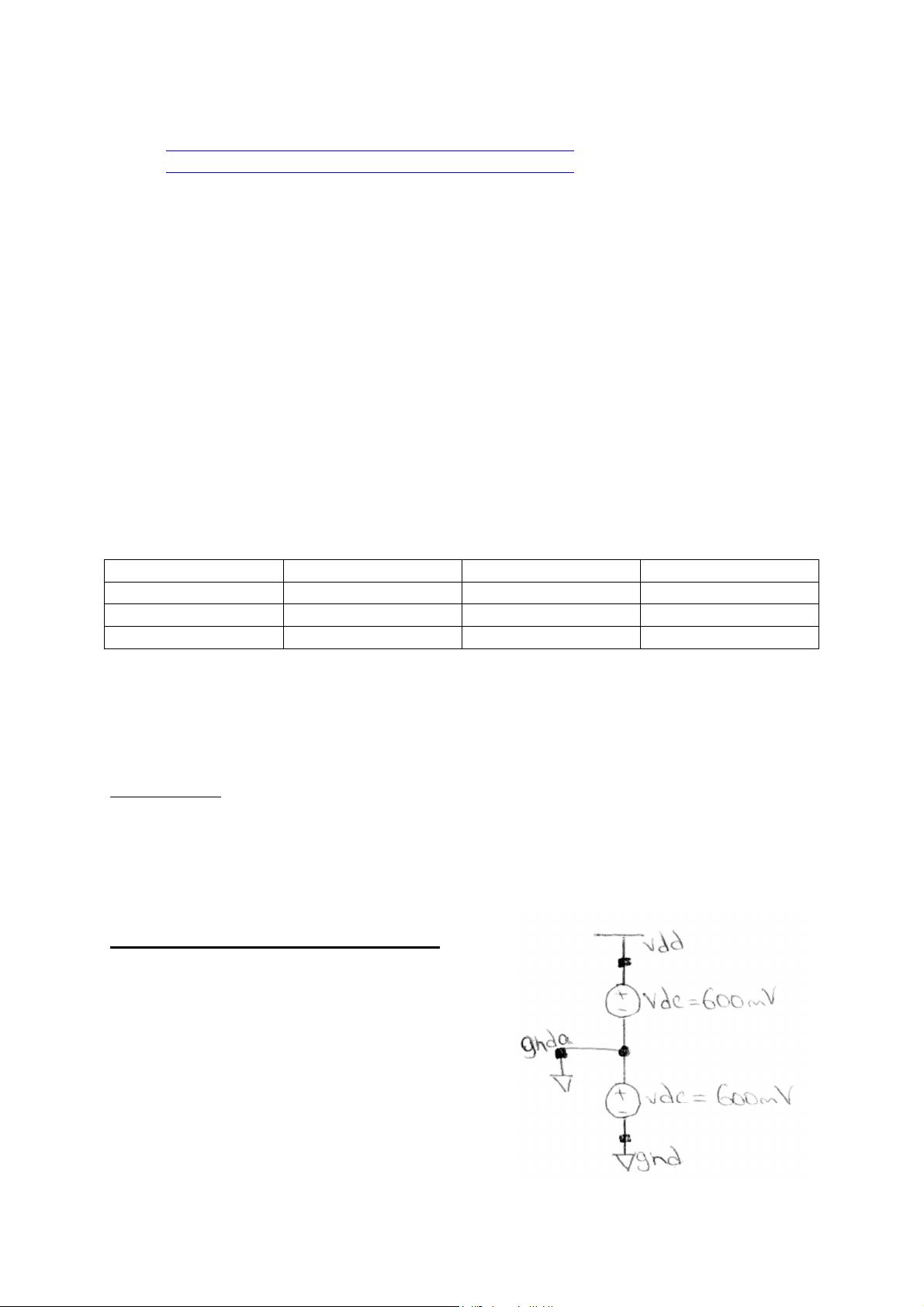
Power supply design for your entire DAC
Use the following diagram for the power supply in
cadence simulations. Make sure all your signals are
centered on the gnda.

bestmyjj
- 粉丝: 0
- 资源: 1
 我的内容管理
收起
我的内容管理
收起
- 我的资源
快来上传第一个资源
 我的收益 登录查看自己的收益
 我的积分
登录查看自己的积分
我的积分
登录查看自己的积分
 我的C币
登录后查看C币余额
我的C币
登录后查看C币余额
 我的收藏
我的收藏  我的下载
我的下载  下载帮助
下载帮助

会员权益专享


最新资源
- 2023年中国辣条食品行业创新及消费需求洞察报告.pptx
- 2023年半导体行业20强品牌.pptx
- 2023年全球电力行业评论.pptx
- 2023年全球网络安全现状-劳动力资源和网络运营的全球发展新态势.pptx
- 毕业设计-基于单片机的液体密度检测系统设计.doc
- 家用清扫机器人设计.doc
- 基于VB+数据库SQL的教师信息管理系统设计与实现 计算机专业设计范文模板参考资料.pdf
- 官塘驿林场林防火(资源监管)“空天地人”四位一体监测系统方案.doc
- 基于专利语义表征的技术预见方法及其应用.docx
- 浅谈电子商务的现状及发展趋势学习总结.doc
- 基于单片机的智能仓库温湿度控制系统 (2).pdf
- 基于SSM框架知识产权管理系统 (2).pdf
- 9年终工作总结新年计划PPT模板.pptx
- Hytera海能达CH04L01 说明书.pdf
- 数据中心运维操作标准及流程.pdf
- 报告模板 -成本分析与报告培训之三.pptx
资源上传下载、课程学习等过程中有任何疑问或建议,欢迎提出宝贵意见哦~我们会及时处理!
点击此处反馈


评论4