
DS07-13703-2E
FUJITSU SEMICONDUCTOR
DATA SHEET
16-bit Proprietary Microcontroller
CMOS
F
2
MC-16LX MB90540/545 Series
MB90F543/F549/V540
■
■■
■
DESCRIPTION
The MB90540/545 series with FULL-CAN*
1
and FLASH ROM is specially designed for automotive and industrial ap-
plications. Its main features are two on board CAN Interfaces (one for MB90V545 series), which conform to V2.0
Part A and Part B, supporting very flexible message buffer
scheme and so offering more functions than a normal
full CAN approach. The instruction set by F
2
MC-16LX CPU core inherits an AT architecture of the F
2
MC*
2
family with
additional instruction sets for high-level languages, extended addressing mode, enhanced multiplication/division in-
structions, and enhanced bit manipulation instructions.The micro controller has a 32-bit accumulator for processing
long word data.The MB90540/545 series has peripheral resources of 8/10-bit A/D converters, UART(SCI), extended
I/O serial interfaces, 8/16-bit timer, I/O timer (input capture(ICU), output compare (OCU)).
*1:Controller Area Network (CAN) - License of Robert Bosch GmbH.
*2:F
2
MC stands for FUJITSU Flexible Microcontroller.
■
■■
■
FEATURES
•Clock
Embedded PLL clock multiplication circuit
Operating clock (PLL clock) can be selected from: divided-by-2 of oscillation or one to four times the oscillation
Minimum instruction execution time: 62.5 ns (operation at oscillation of 4 MHz, four times the oscillation clock,
V
CC of 5.0V)
Subsystem Clock: 32 kHz
(Continued)
■
■■
■
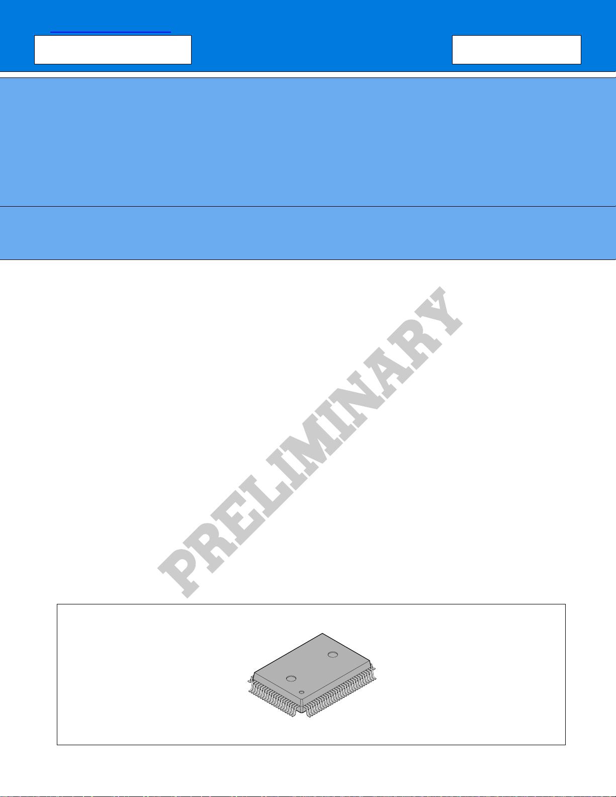
PACKAGE
100-pin Plastic QFP
(FPT-100P-M06)
查询MB90F546G供应商


剩余55页未读,继续阅读

yuefeifei10010
- 粉丝: 0
- 资源: 1
 我的内容管理
收起
我的内容管理
收起
- 我的资源
快来上传第一个资源
 我的收益 登录查看自己的收益
 我的积分
登录查看自己的积分
我的积分
登录查看自己的积分
 我的C币
登录后查看C币余额
我的C币
登录后查看C币余额
 我的收藏
我的收藏  我的下载
我的下载  下载帮助
下载帮助

会员权益专享


最新资源
- 数据结构1800题含完整答案详解.doc
- 医疗企业薪酬系统设计与管理方案.pptx
- 界面与表面技术界面理论与表面技术要点PPT学习教案.pptx
- Java集合排序及java集合类详解(Collection、List、Map、Set)讲解.pdf
- 网页浏览器的开发 (2).pdf
- 路由器原理与设计讲稿6-交换网络.pptx
- 火电厂锅炉过热汽温控制系统设计.doc
- 企业识别CIS系统手册[收集].pdf
- 物业管理基础知识.pptx
- 第4章财务预测.pptx
- 《集成电路工艺设计及器件特性分析》——实验教学计算机仿真系.pptx
- 局域网内共享文件提示没有访问权限的问题借鉴.pdf
- 第5章网络营销策略.pptx
- 固井质量测井原理PPT教案.pptx
- 毕业实习总结6篇.doc
- UGNX建模基础篇草图模块PPT学习教案.pptx
资源上传下载、课程学习等过程中有任何疑问或建议,欢迎提出宝贵意见哦~我们会及时处理!
点击此处反馈


评论0