
2
PCM5100A
,
PCM5101A
,
PCM5102A
PCM5100A-Q1
,
PCM5101A-Q1
,
PCM5102A-Q1
ZHCSA60C –MAY 2012–REVISED MAY 2015
www.ti.com.cn
版权 © 2012–2015, Texas Instruments Incorporated
目目录录
1 特特性性.......................................................................... 1
2 应应用用.......................................................................... 1
3 说说明明.......................................................................... 1
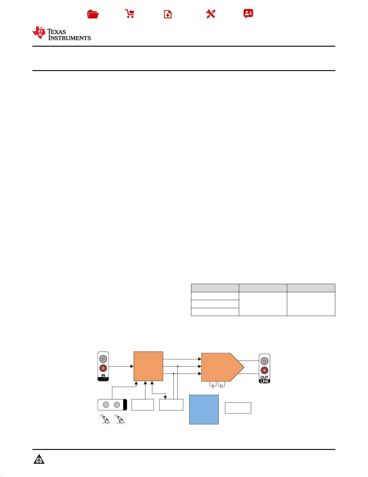
4 简简化化系系统统图图............................................................... 1
5 修修订订历历史史记记录录 ........................................................... 2
6 Device Comparison ............................................... 4
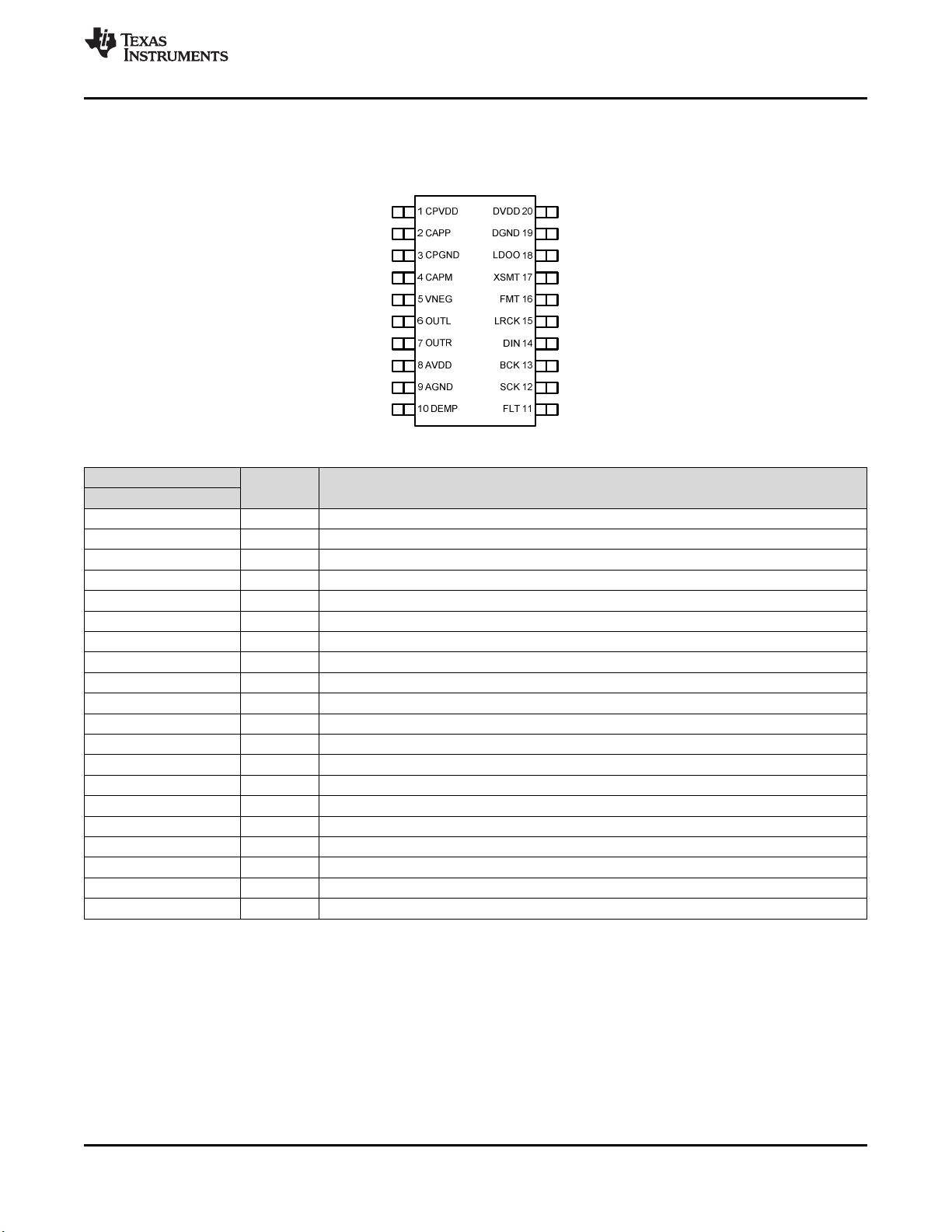
7 Pin Configuration and Functions......................... 5
8 Specifications......................................................... 6
8.1 Absolute Maximum Ratings ...................................... 6
8.2 ESD Ratings ............................................................ 6
8.3 Recommended Operating Conditions....................... 6
8.4 Thermal Information.................................................. 6
8.5 Electrical Characteristics........................................... 7
8.6 Timing Requirements.............................................. 11
8.7 Timing Requirements, XSMT.................................. 11
8.8 Typical Characteristics............................................ 12
9 Detailed Description............................................ 14
9.1 Overview ................................................................. 14
9.2 Functional Block Diagram ....................................... 14
9.3 Feature Description................................................. 14
9.4 Device Functional Modes........................................ 25
10 Applications and Implementation...................... 26
10.1 Application Information.......................................... 26
11 Power Supply Recommendations ..................... 28
11.1 Power Supply Distribution and Requirements ...... 28
11.2 Recommended Powerdown Sequence................. 28
11.3 External Power Sense Undervoltage Protection
Mode ........................................................................ 30
11.4 Power-On Reset Function..................................... 32
11.5 PCM510xA Power Modes..................................... 33
12 Layout................................................................... 34
12.1 Layout Guidelines ................................................. 34
13 器器件件和和文文档档支支持持 ..................................................... 35
13.1 相关链接................................................................ 35
13.2 社区资源................................................................ 35
13.3 商标 ....................................................................... 35
13.4 静电放电警告......................................................... 35
14 机机械械、、封封装装和和可可订订购购信信息息....................................... 35
14.1 机械数据................................................................ 35
5 修修订订历历史史记记录录
注:之前版本的页码可能与当前版本有所不同。
Changes from Revision B (January 2015) to Revision C Page
• 已更改
简化系统图
.................................................................................................................................................................. 1
• Changed typical performance table to reflect part differences accurately ............................................................................ 4
• Changed "Storage temperatures, T
stg
" to "Operating junction temperature range at –40°C to 130°C" ................................. 6
• Changed "Storage temperature (Q1 devices) –40°C to 125°C" to "Storage temperatures, T
stg
–65°C to 150°C" ................ 6
• Changed the stereo line output load resistance MIN value in the Recommended Operating Conditions from "2 kΩ"
to "1 kΩ".................................................................................................................................................................................. 6
• Changed the operating junction temperature range in the Recommended Operating Conditions from "MIN = –25°C
MAX = 85°C" to "MIN = –40°C MAX = 130°C"....................................................................................................................... 6
• Added "Q1 Automotive grade devices... " and " Consumer grade (non-Q1) devices..." to the condition statement in
the Electrical Characteristics .................................................................................................................................................. 7
• Added "Q1 Automotive grade devices... " and " Consumer grade (non-Q1) devices..." to the condition statement in
the Typical Characteristics graphs section........................................................................................................................... 12
• 已更改 "MCK" to "SCK" at the PLL Clock in the Functional Block Diagram ........................................................................ 14
• Added label "Mute Circuit" and ground symbols to pins DEMP and FMT in Figure 33 ...................................................... 26
Changes from Revision A (September 2012) to Revision B Page
• 已添加 ESD
额定值
表,
详细 说明
部分,
应用和实施
部分,
电源相关建议
部分,
器件和文档支持
部分以及
机械、封装
和可订购信息
.......................................................................................................................................................................... 1
• 已添加 1.8V DVDD 电源项 ..................................................................................................................................................... 1
• 已更改
特性
列表。 .................................................................................................................................................................. 1
• Changed "Operating temperature range " to "Operating junction temperature range" .......................................................... 6
• Deleted redundant PLL specification in the Recommended Operating Conditions .............................................................. 6
• 已删除 "Intelligent clock error..." and "...for pop-free performance." .................................................................................... 14
• Clarified clock generation explanation.................................................................................................................................. 24


 我的内容管理
收起
我的内容管理
收起
 我的收益 登录查看自己的收益
 我的积分
登录查看自己的积分
我的积分
登录查看自己的积分
 我的C币
登录后查看C币余额
我的C币
登录后查看C币余额
 我的收藏
我的收藏  我的下载
我的下载  下载帮助
下载帮助 


评论0