没有合适的资源?快使用搜索试试~ 我知道了~
首页MCP2515 芯片手册
MCP2515 芯片手册
5星 · 超过95%的资源 需积分: 49 25 下载量 30 浏览量
更新于2023-03-16
评论
收藏 1.02MB PDF 举报
Microchip 的MCP2515 是一款独立控制器局域网络(Controller Area Network, CAN)协议控制器,完全支持CAN V2.0B 技术规范。该器件能发送和接收标准和扩展数据帧以及远程帧。MCP2515 自带的两个验收屏蔽寄存器和六个验收滤波寄存器可以过滤掉不想要的报文,因此减少了主单片机(MCU)的开销。MCP2515与MCU 的连接是通过业界标准串行外设接口(Serial Peripheral Interface, SPI)来实现的。
资源详情
资源评论
资源推荐
© 2005 Microchip Technology Inc. Preliminary DS21801D-page 1
MCP2515
Features
• Implements CAN V2.0B at 1 Mb/s:
- 0 – 8 byte length in the data field
- Standard and extended data and remote
frames
• Receive buffers, masks and filters:
- Two receive buffers with prioritized message
storage
- Six 29-bit filters
-Two 29-bit masks
• Data byte filtering on the first two data bytes
(applies to standard data frames)
• Three transmit buffers with prioritizaton and abort
features
• High-speed SPI™ Interface (10 MHz):
- SPI modes 0,0 and 1,1
• One-shot mode ensures message transmission is
attempted only one time
• Clock out pin with programmable prescaler:
- Can be used as a clock source for other
device(s)
• Start-of-Frame (SOF) signal is available for
monitoring the SOF signal:
- Can be used for time-slot-based protocols
and/or bus diagnostics to detect early bus
degredation
• Interrupt output pin with selectable enables
• Buffer Full output pins configurable as:
- Interrupt output for each receive buffer
- General purpose output
• Request-to-Send (RTS) input pins individually
configurable as:
- Control pins to request transmission for each
transmit buffer
- General purpose inputs
• Low-power CMOS technology:
- Operates from 2.7V – 5.5V
- 5 mA active current (typical)
- 1 µA standby current (typical) (Sleep mode)
• Temperature ranges supported:
- Industrial (I): -40°C to +85°C
- Extended (E): -40°C to +125°C
Description
Microchip Technology’s MCP2515 is a stand-alone
Controller Area Network (CAN) controller that imple-
ments the CAN specification, version 2.0B. It is capable
of transmitting and receiving both standard and
extended data and remote frames. The MCP2515 has
two acceptance masks and six acceptance filters that
are used to filter out unwanted messages, thereby
reducing the host MCUs overhead. The MCP2515
interfaces with microcontrollers (MCUs) via an industry
standard Serial Peripheral Interface (SPI).
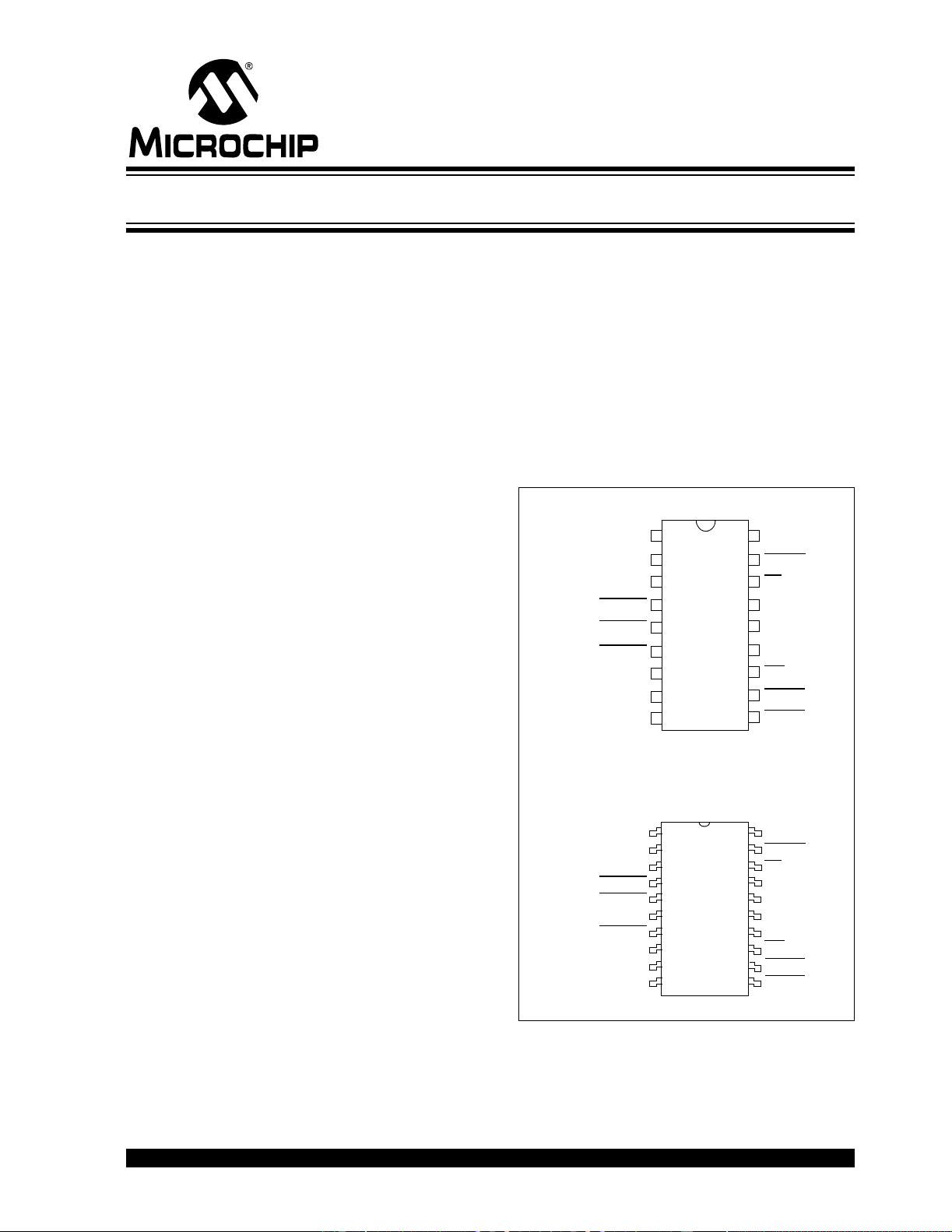
Package Types
TXCAN
RXCAN
V
DD
RESET
CS
SO
MCP2515
1
2
3
4
18
17
16
15
SI
SCK
INT
RX0BF
14
13
12
11
RX1BF
10
OSC2
OSC1
CLKOUT/SOF
TX2RTS
5
6
7
8
Vss
9
TX0RTS
TX1RTS
MCP2515
TXCAN
RXCAN
TX0RTS
OSC1
CLKOUT/SOF
OSC2
CS
VDD
RESET
SO
SCK
INT
SI
RX0BF
RX1BF
VSS
TX1RTS
TX2RTS
NC
NC
13
12
1
2
3
4
5
6
7
8
9
20
19
18
17
16
15
14
11
10
18-Lead PDIP/SOIC
20-LEAD TSSOP
Stand-Alone CAN Controller With SPI™ Interface
MCP2515
DS21801D-page 2 Preliminary © 2005 Microchip Technology Inc.
NOTES:
© 2005 Microchip Technology Inc. Preliminary DS21801D-page 3
MCP2515
1.0 DEVICE OVERVIEW
The MCP2515 is a stand-alone CAN controller
developed to simplify applications that require
interfacing with a CAN bus. A simple block diagram of
the MCP2515 is shown in Figure 1-1. The device
consists of three main blocks:
1. The CAN module, which includes the CAN
protocol engine, masks, filters, transmit and
receive buffers.
2. The control logic and registers that are used to
configure the device and its operation.
3. The SPI protocol block.
An example system implementation using the device is
shown in Figure 1-2.
1.1 CAN Module
The CAN module handles all functions for receiving
and transmitting messages on the CAN bus. Messages
are transmitted by first loading the appropriate
message buffer and control registers. Transmission is
initiated by using control register bits via the SPI
interface or by using the transmit enable pins. Status
and errors can be checked by reading the appropriate
registers. Any message detected on the CAN bus is
checked for errors and then matched against the user-
defined filters to see if it should be moved into one of
the two receive buffers.
1.2 Control Logic
The control logic block controls the setup and operation
of the MCP2515 by interfacing to the other blocks in
order to pass information and control.
Interrupt pins are provided to allow greater system
flexibility. There is one multi-purpose interrupt pin (as
well as specific interrupt pins) for each of the receive
registers that can be used to indicate a valid message
has been received and loaded into one of the receive
buffers. Use of the specific interrupt pins is optional.
The general purpose interrupt pin, as well as status
registers (accessed via the SPI interface), can also be
used to determine when a valid message has been
received.
Additionally, there are three pins available to initiate
immediate transmission of a message that has been
loaded into one of the three transmit registers. Use of
these pins is optional, as initiating message
transmissions can also be accomplished by utilizing
control registers, accessed via the SPI interface.
1.3 SPI Protocol Block
The MCU interfaces to the device via the SPI interface.
Writing to, and reading from, all registers is
accomplished using standard SPI read and write
commands, in addition to specialized SPI commands.
FIGURE 1-1: BLOCK DIAGRAM
SPI™
Interface
Logic
SPI
Bus
INT
CS
SCK
SI
SO
CAN
Protocol
Engine
RXCAN
TXCAN
Control Logic
RX0BF
RX1BF
TX0RTS
TX1RTS
TX2RTS
TX and RX Buffers
Masks and Filters
CAN Module
RESET
Timing
Generation
OSC1
OSC2
CLKOUT
Control
and
Interrupt
Registers
MCP2515
DS21801D-page 4 Preliminary © 2005 Microchip Technology Inc.
FIGURE 1-2: EXAMPLE SYSTEM IMPLEMENTATION
TABLE 1-1: PINOUT DESCRIPTION
Name
PDIP/SOIC
Pin #
TSSOP
Pin #
I/O/P
Type
Description Alternate Pin Function
TXCAN 1 1 O Transmit output pin to CAN bus —
RXCAN 2 2 I Receive input pin from CAN bus —
CLKOUT 3 3 O Clock output pin with programmable
prescaler
Start-of-Frame signal
TX0RTS
4 4 I Transmit buffer TXB0 request-to-send.
100 kΩ internal pull-up to V
DD
General purpose digital input.
100 kΩ internal pull-up to V
DD
TX1RTS 5 5 I Transmit buffer TXB1 request-to-send.
100 kΩ internal pull-up to V
DD
General purpose digital input.
100 kΩ internal pull-up to V
DD
TX2RTS 6 7 I Transmit buffer TXB2 request-to-send.
100 kΩ internal pull-up to V
DD
General purpose digital input.
100 kΩ internal pull-up to V
DD
OSC2 7 8 O Oscillator output —
OSC1 8 9 I Oscillator input External clock input
V
SS 9 10 P Ground reference for logic and I/O pins —
RX1BF
10 11 O Receive buffer RXB1 interrupt pin or
general purpose digital output
General purpose digital output
RX0BF
11 12 O Receive buffer RXB0 interrupt pin or
general purpose digital output
General purpose digital output
INT
12 13 O Interrupt output pin —
SCK 13 14 I Clock input pin for SPI™ interface —
SI 14 16 I Data input pin for SPI interface —
SO 15 17 O Data output pin for SPI interface —
CS 16 18 I Chip select input pin for SPI interface —
RESET 17 19 I Active low device reset input —
VDD 18 20 P Positive supply for logic and I/O pins —
NC — 6,15 — No internal connection
Note: Type Identification: I = Input; O = Output; P = Power
Node
Controller
MCP2515
XCVR
SPI™
TX
RX
CANH
CANL
Node
Controller
MCP2515
XCVR
SPI
TX
RX
Node
Controller
MCP2515
XCVR
SPI
TX
RX
© 2005 Microchip Technology Inc. Preliminary DS21801D-page 5
MCP2515
1.4 Transmit/Receive
Buffers/Masks/Filters
The MCP2515 has three transmit and two receive
buffers, two acceptance masks (one for each receive
buffer) and a total of six acceptance filters. Figure 1-3
shows a block diagram of these buffers and their
connection to the protocol engine.
FIGURE 1-3: CAN BUFFERS AND PROTOCOL ENGINE BLOCK DIAGRAM
Acceptance Filter
RXF2
R
X
B
1
Identifier
Data Field Data Field
Identifier
Acceptance Mask
RXM1
Acceptance Filter
RXF3
Acceptance Filter
RXF4
Acceptance Filter
RXF5
M
A
B
Acceptance Filter
RXF0
Acceptance Filter
RXF1
R
X
B
0
TXREQ
TXB2
ABTF
MLOA
TXERR
MESSAGE
Message
Queue
Control
Transmit Byte Sequencer
TXREQ
TXB0
ABTF
MLOA
TXERR
MESSAGE
CRC<14:0>
Comparator
Receive<7:0>Transmit<7:0>
Receive
Error
Transmit
Error
Protocol
REC
TEC
ErrPas
BusOff
Finite
State
Machine
Counter
Counter
Shift<14:0>
{Transmit<5:0>, Receive<8:0>}
Transmit
Logic
Bit
Timing
Logic
TX RX
Configuration
Registers
Clock
Generator
PROTOCOL
ENGINE
BUFFERS
TXREQ
TXB1
ABTF
MLOA
TXERR
MESSAGE
Acceptance Mask
RXM0
A
c
c
e
p
t
A
c
c
e
p
t
SOF
剩余83页未读,继续阅读
weixin_40290325
- 粉丝: 0
- 资源: 2
上传资源 快速赚钱
- 我的内容管理 收起
- 我的资源 快来上传第一个资源
- 我的收益 登录查看自己的收益
- 我的积分 登录查看自己的积分
- 我的C币 登录后查看C币余额
- 我的收藏
- 我的下载
- 下载帮助
会员权益专享
最新资源
- c++校园超市商品信息管理系统课程设计说明书(含源代码) (2).pdf
- 建筑供配电系统相关课件.pptx
- 企业管理规章制度及管理模式.doc
- vb打开摄像头.doc
- 云计算-可信计算中认证协议改进方案.pdf
- [详细完整版]单片机编程4.ppt
- c语言常用算法.pdf
- c++经典程序代码大全.pdf
- 单片机数字时钟资料.doc
- 11项目管理前沿1.0.pptx
- 基于ssm的“魅力”繁峙宣传网站的设计与实现论文.doc
- 智慧交通综合解决方案.pptx
- 建筑防潮设计-PowerPointPresentati.pptx
- SPC统计过程控制程序.pptx
- SPC统计方法基础知识.pptx
- MW全能培训汽轮机调节保安系统PPT教学课件.pptx
资源上传下载、课程学习等过程中有任何疑问或建议,欢迎提出宝贵意见哦~我们会及时处理!
点击此处反馈
安全验证
文档复制为VIP权益,开通VIP直接复制
信息提交成功
评论1