没有合适的资源?快使用搜索试试~ 我知道了~
首页DDR4 UDIM Design specification
资源详情
资源评论
资源推荐
COMMITTEE LETTER BALLOT
Solid State Technology Association
3103 North 10th Street
Arlington, Virginia 22201
Ballot Template Version draft rev. 5/16
© JEDEC 2011
Committee: JC45.3
Committee Item Number: 2231.16
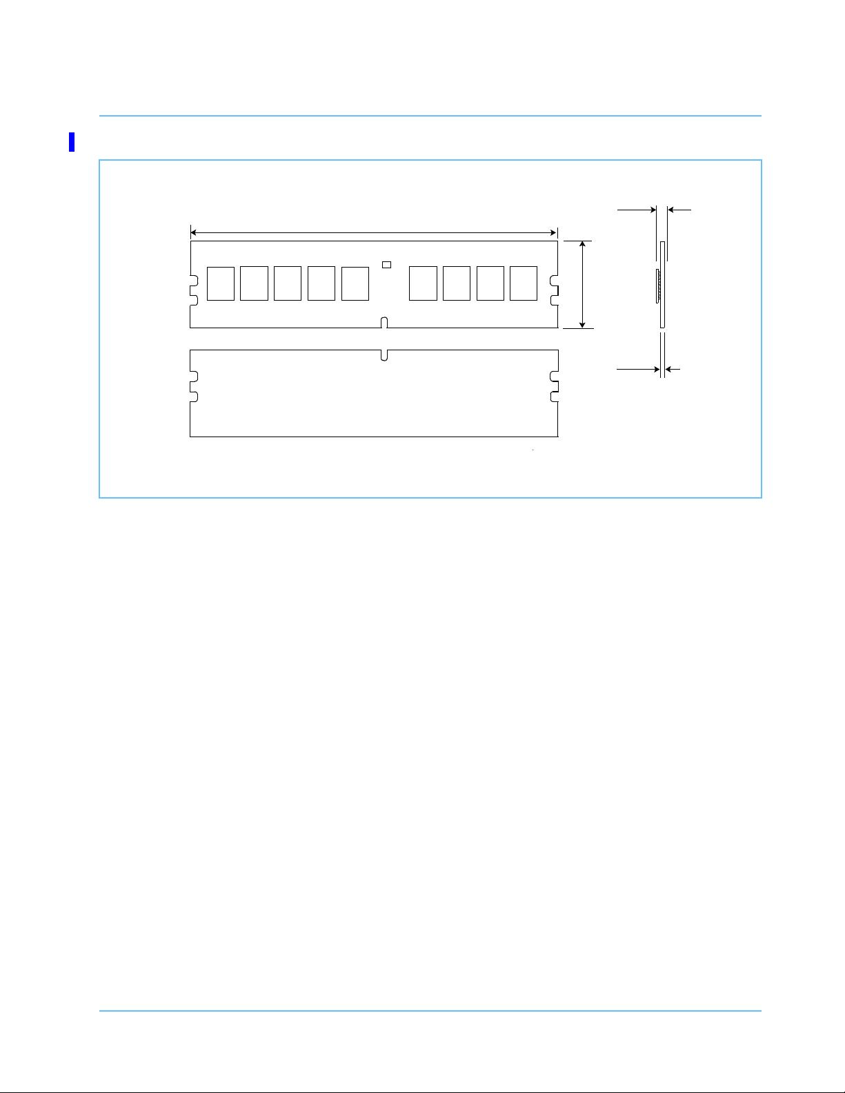
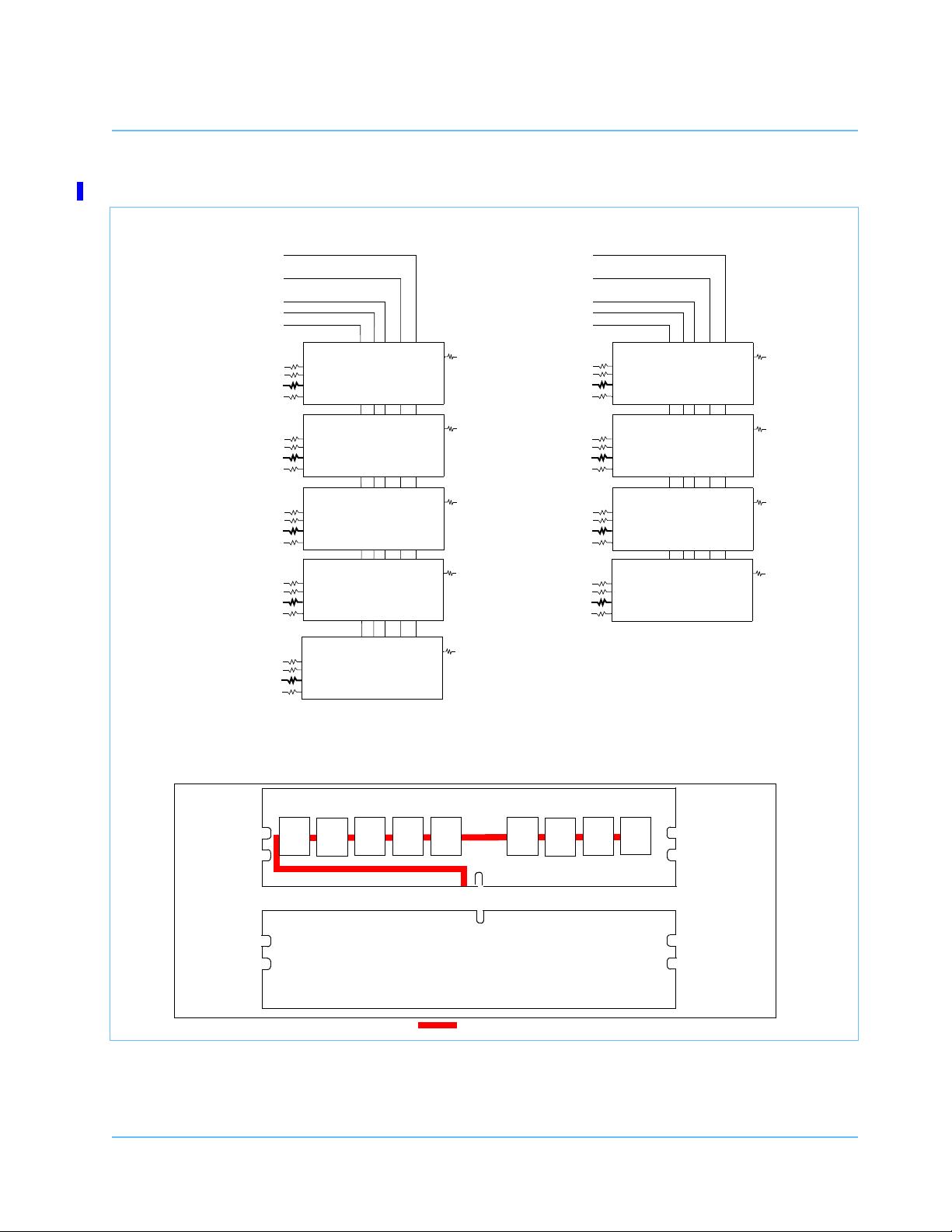
Subject: Proposed DDR4 UDIMM Design Specification Annex-D
Background: At the March committee meeting, the DDR4 UDIMM taskgroup was re-
authorized to ballot the DDR4 R/C D1 ECC 1Rx8 based UDIMM specifi-
cation annex and registration. This is the ballot for the UDIMM R/C D1
design annex.
Keywords: DDR4, UDIMM, R/C D1, Design Specification
Page D1 Revision 1.90
DDR4 UDIMM Design Specification Annex-D
Annex D - Raw Card D JEDEC internal use only
Proposed
Annex D - Raw Card D
DDR4 Unbuffered DIMM Design File
Raw Card Applicable Design File Applicable BOM
D0 PC4-UDIMM_V080_RC_D0_20131028.brd
PC4-UDIMM_V080_RC_D0_20131028_BOM.xlsx
D1 PC4-UDIMM_V191_RC_A1_D1_20150424.brd
PC4-UDIMM_V191_RC_D1_20150424_BOM.xlsx
Note: “Reference” design file updates will be released as needed. This DIMM specification will reflect the most recent design files, but
may also be updated to reflect clarifications to the specification only. In these cases the design files will not be updated.
Module Configuration
DIMM SDRAM
# of
SDRAM die
(Min/Max)
# of Logical
Ranks per
DIMM
(Min/Max)
# of Package
Ranks per
DIMM
(Min/Max)
# of Address bits
(row/col)
MO-309
variation
Maximum
Capacity
Organization Die Density Organization
2 GB 256 Mb x72 2 Gb
256 Mb x 8
9 / 9
11
14 / 10
1
AAxA
4 GB 512 Mb x72 4 Gb
512 Mb x 8
9 / 9
11
15 / 10
1
AAxA
8 GB 1 Gb x72 8 Gb
1 Gb x 8
9 / 9
1 1 16 / 10 AAxA
16 GB 2 Gb x72 16 Gb
2 Gb x 8
9 / 9
1 1 17 / 10 AAxA
1. Address A16 is the highest address bit used based on it being multiplexed with RAS_n
SDRAM Configuration
Supported DRAM Outline
(Width x Length) nom.
# of Banks in
SDRAM
BA/BG
SDRAM
Package Type
Package Type
MO-207
variation
11.0 x 13.0 (mm)
2 / 2 78 Ball FBGA
SDP
DW-z
Note: SDP is a Single Die per Package.
Supported Speeds
Raw Card Speed PC4-1333 PC4-1600 PC4-1866 PC4-2133 PC4-2400 PC4-2666 PC4-3200 Notes
D0DDR4XXXX
1, 2
D1DDR4NNNNN
1, 2
Note 1: X reflects speed grades approved from previous ballots.
Note 2: N denotes speed grades being proposed for this most recent ballot
Design Deviations
1. None.
DDR4 UDIMM Design Specification Annex-D
General Layout JEDEC internal use only
Revision 1.90 Page D2
Proposed
General Layout
Note 1: Refer to MO-309 for more detailed information.
Note 2: Variation is AAxA (A Module height, A Moduile thickness, x plating, A Key Position).
Note 3: Module thickness may vary with DRAM thickness and passive components.
1.4
133.35
31.25
3.9 Max
Back
Front
Side
Page D3 Revision 1.90
DDR4 UDIMM Design Specification Annex-D
Functional Block Diagram JEDEC internal use only
Proposed
Functional Block Diagram
Note 1: CK1
_t
, CK1
_c
terminated with 120 ± 5% resistor.
Note 2: Unless otherwise noted resistors are 15 ± 5%.
Note 3: ZQ resistors are 240 ± 1%. For all other resistor values refer to the appropriate wiring diagram.
Note 4: Event_n is used for SPD with TS. Option Resistor for it should be placed.
x72 DIMM, populated as one package rank of x8 DDR4 SDRAMs (Part 1 of 1)
Address, Command and Control lines
Back
Front
D1
D3
D5
D7
D0
D2
D4
D6
D8
CK0_t,CK0_c
A[16:0],BA[1:0],
DQ [7:0]
DQS0_t
DQS0_c
DQ [15:8]
DQS1_t
DQS1_c
DQ [23:16]
DQS2_t
DQS2_c
DQ [31:24]
DQS3_t
DQS3_c
CKE0
ODT0
CS0_n
D0
DQS_c
DQS_t
C
K
E
C
S
_
n
DQ [7:0]
O
D
T
ZQ
VSS
ACT_n,PARITY,BG[1:0]
A
d
d
r
e
s
s
C
K
DBI_n/DM_n
DBI0_n, DM0_n
D1
DQS_c
DQS_t
C
K
E
C
S
_
n
DQ [7:0]
O
D
T
ZQ
VSS
A
d
d
r
e
s
s
C
K
DBI_n/DM_n
DBI1_n, DM1_n
D2
DQS_c
DQS_t
C
K
E
C
S
_
n
DQ [7:0]
O
D
T
ZQ
VSS
A
d
d
r
e
s
s
C
K
DBI_n/DM_n
DBI2_n, DM2_n
D3
DQS_c
DQS_t
C
K
E
C
S
_
n
DQ [7:0]
O
D
T
ZQ
VSS
A
d
d
r
e
s
s
C
K
DBI_n/DM_n
DBI3_n, DM3_n
CK0_t,CK0_c
A[16:0],BA[1:0],
CKE0
ODT0
CS0_n
D4
DQS_c
DQS_t
C
K
E
C
S
_
n
DQ [7:0]
O
D
T
ZQ
VSS
ACT_n,PARITY,BG[1:0]
A
d
d
r
e
s
s
C
K
DBI_n/DM_n
D5
DQS_c
DQS_t
C
K
E
C
S
_
n
DQ [7:0]
O
D
T
ZQ
VSS
A
d
d
r
e
s
s
C
K
DBI_n/DM_n
D6
DQS_c
DQS_t
C
K
E
C
S
_
n
DQ [7:0]
O
D
T
ZQ
VSS
A
d
d
r
e
s
s
C
K
DBI_n/DM_n
D7
DQS_c
DQS_t
C
K
E
C
S
_
n
DQ [7:0]
O
D
T
ZQ
VSS
A
d
d
r
e
s
s
C
K
DBI_n/DM_n
DQ [39:32]
DQS4_t
DQS4_c
DQ [47:40]
DQS5_t
DQS5_c
DQ [55:48]
DQS6_t
DQS6_c
DQ [63:56]
DQS7_t
DQS7_c
DBI4_n, DM4_n
DBI5_n, DM5_n
DBI6_n, DM6_n
DBI7_n, DM7_n
DQ [71:64]
DQS8_t
DQS8_c
D8
DQS_c
DQS_t
C
K
E
C
S
_
n
DQ [7:0]
O
D
T
ZQ
VSS
A
d
d
r
e
s
s
C
K
DBI_n/DM_n
DBI8_n, DM8_n
剩余16页未读,继续阅读
farfong
- 粉丝: 1
- 资源: 7
上传资源 快速赚钱
- 我的内容管理 收起
- 我的资源 快来上传第一个资源
- 我的收益 登录查看自己的收益
- 我的积分 登录查看自己的积分
- 我的C币 登录后查看C币余额
- 我的收藏
- 我的下载
- 下载帮助
会员权益专享
最新资源
- RTL8188FU-Linux-v5.7.4.2-36687.20200602.tar(20765).gz
- c++校园超市商品信息管理系统课程设计说明书(含源代码) (2).pdf
- 建筑供配电系统相关课件.pptx
- 企业管理规章制度及管理模式.doc
- vb打开摄像头.doc
- 云计算-可信计算中认证协议改进方案.pdf
- [详细完整版]单片机编程4.ppt
- c语言常用算法.pdf
- c++经典程序代码大全.pdf
- 单片机数字时钟资料.doc
- 11项目管理前沿1.0.pptx
- 基于ssm的“魅力”繁峙宣传网站的设计与实现论文.doc
- 智慧交通综合解决方案.pptx
- 建筑防潮设计-PowerPointPresentati.pptx
- SPC统计过程控制程序.pptx
- SPC统计方法基础知识.pptx
资源上传下载、课程学习等过程中有任何疑问或建议,欢迎提出宝贵意见哦~我们会及时处理!
点击此处反馈
安全验证
文档复制为VIP权益,开通VIP直接复制
信息提交成功
评论0