Solutions
1
Solutions for CMOS VLSI Design 4th Edition. Last updated 12 May 2010.
Chapter 1
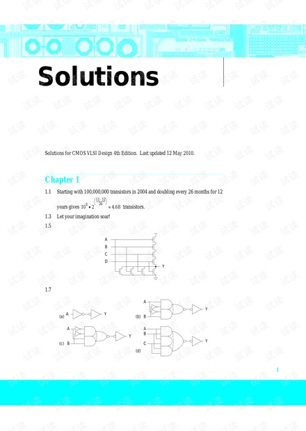
1.1 Starting with 100,000,000 transistors in 2004 and doubling every 26 months for 12
years gives transistors.
1.3 Let your imagination soar!
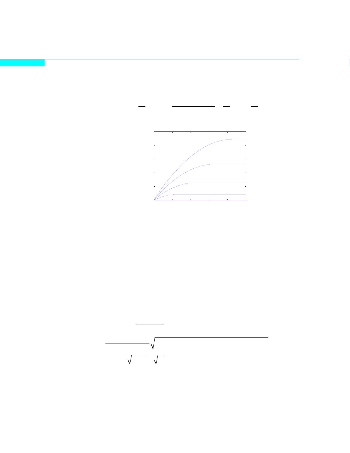
1.5
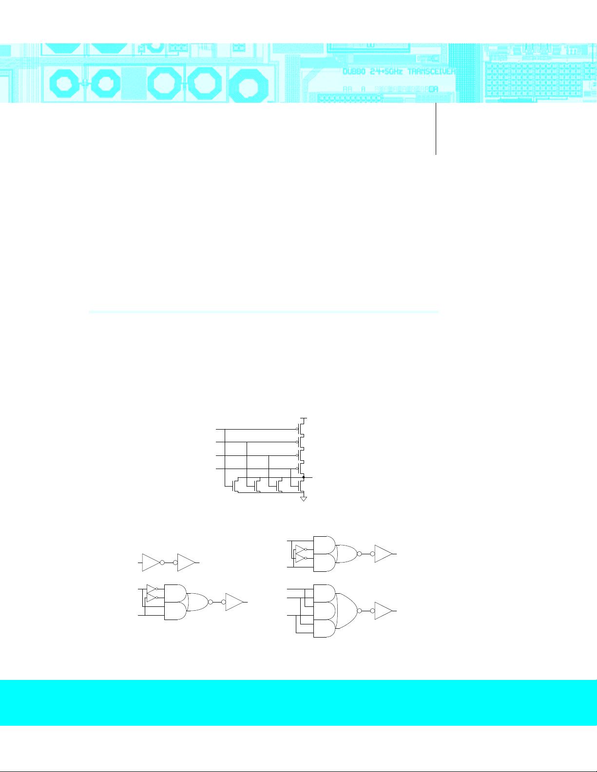
1.7
10
8
2
12 12⋅
26
----------------
⎝⎠
⎛⎞
• 4.6B≈
A
B
C
D
Y
AY
(a)
A
B
Y
(b)
A
B
Y
(c)
(d)
A
C
B
Y

剩余38页未读,继续阅读

Arffy
- 粉丝: 0
- 资源: 2
 我的内容管理
收起
我的内容管理
收起
- 我的资源
快来上传第一个资源
 我的收益 登录查看自己的收益
 我的积分
登录查看自己的积分
我的积分
登录查看自己的积分
 我的C币
登录后查看C币余额
我的C币
登录后查看C币余额
 我的收藏
我的收藏  我的下载
我的下载  下载帮助
下载帮助

会员权益专享


最新资源
- 2023年中国辣条食品行业创新及消费需求洞察报告.pptx
- 2023年半导体行业20强品牌.pptx
- 2023年全球电力行业评论.pptx
- 2023年全球网络安全现状-劳动力资源和网络运营的全球发展新态势.pptx
- 毕业设计-基于单片机的液体密度检测系统设计.doc
- 家用清扫机器人设计.doc
- 基于VB+数据库SQL的教师信息管理系统设计与实现 计算机专业设计范文模板参考资料.pdf
- 官塘驿林场林防火(资源监管)“空天地人”四位一体监测系统方案.doc
- 基于专利语义表征的技术预见方法及其应用.docx
- 浅谈电子商务的现状及发展趋势学习总结.doc
- 基于单片机的智能仓库温湿度控制系统 (2).pdf
- 基于SSM框架知识产权管理系统 (2).pdf
- 9年终工作总结新年计划PPT模板.pptx
- Hytera海能达CH04L01 说明书.pdf
- 数据中心运维操作标准及流程.pdf
- 报告模板 -成本分析与报告培训之三.pptx
资源上传下载、课程学习等过程中有任何疑问或建议,欢迎提出宝贵意见哦~我们会及时处理!
点击此处反馈


评论3