没有合适的资源?快使用搜索试试~ 我知道了~
首页TN4040_DDR4_Point_to_Point_Design_Guide.pdf
TN4040_DDR4_Point_to_Point_Design_Guide.pdf
需积分: 9 32 下载量 65 浏览量
更新于2023-03-16
评论 1
收藏 866KB PDF 举报
ddr4电路设计走线指导书:DDR4 memory systems are quite similar to DDR3 memory systems. However, there are several noticeable and important changes required by DDR4 that directly affect the board’s design:
资源详情
资源评论
资源推荐
Technical Note
DDR4 Point-to-Point Design Guide
Introduction
DDR4 memory systems are quite similar to DDR3 memory systems. However, there are
several noticeable and important changes required by DDR4 that directly affect the
board’s design:
• New V
PP
supply
• Removed V
REFDQ
reference input
• Changed I/O buffer interface from midpoint terminated SSTL to V
DD
terminated
pseudo open-drain (POD)
• Added ACT_n control
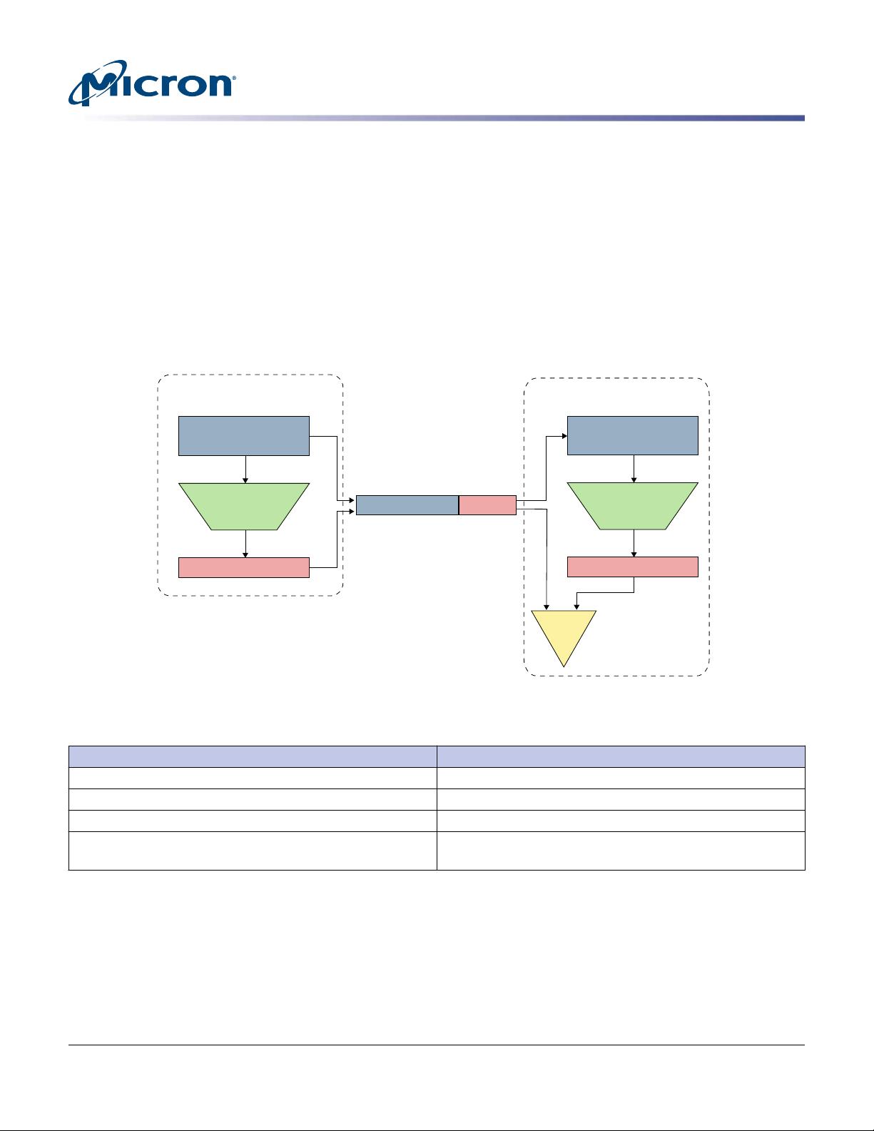
DDR4 added over 30 new features with a significant number of them offering improved
signaling or debug capabilities: CA parity, multipurpose register, programmable write
preamble, programmable read preamble, read preamble training, write CRC, read DBI,
write DBI, V
REFDQ
calibration, and per DRAM addressability. It is beyond the scope of
this document to provide an in-depth explanation of these features; however, a success-
ful DDR4 high-speed design will require the use of these new features and they should
not be overlooked. The Micron DDR4 data sheet provides in-depth explanation of these
features.
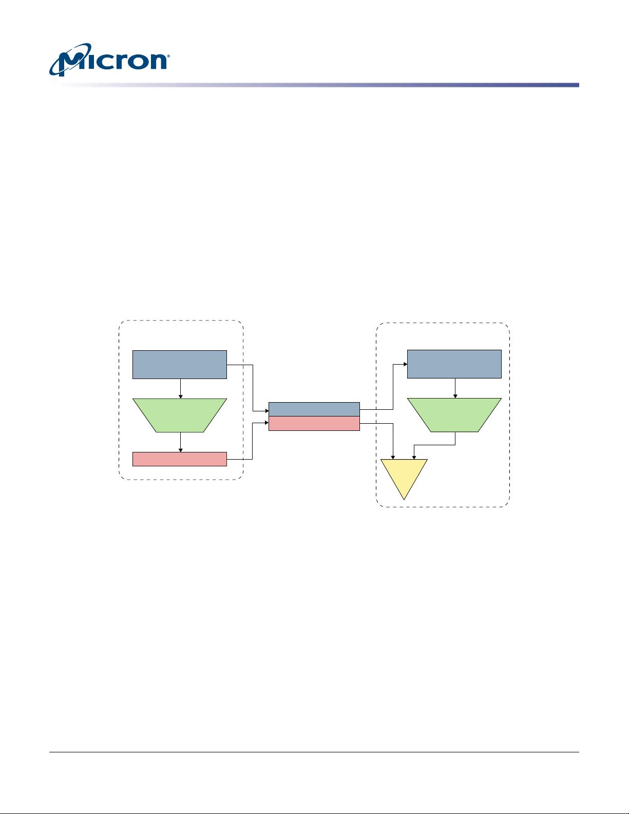
As the DRAM’s operating clock rates have steadily increased, doubling with each DDR
technology increment, DRAM training/calibration has gone from being a luxury in DDR
to being an absolute necessity with DDR4. For example, if the required V
REFDQ
calibra-
tion and data bus write training were not correctly performed, DDR4 timing specifica-
tions would have to be severely derated; but the issue is moot since the specifications
require V
REFDQ
calibration and data bus write training.
The first section of this document highlights some new DDR4 features that can help en-
able a successful board operation and debug. These features offer the potential for im-
proved system performance and increased bandwidth over DDR3 devices for system
designers who are able to properly design around the timing constraints introduced by
this technology. The second section outlines a set of board design rules, providing a
starting point for a board design. And the third section details the calculation process
for determining the portion of the total timing budget allotted to the board intercon-
nect. The intent is that board designers will use the first section to develop a set of gen-
eral rules and then, through simulation, verify their designs in the intended environ-
ment.
The suggestions provided in this technical note mitigating
t
RC,
t
RRD,
t
FAW,
t
CCD, and
t
WTR can help system designers optimize DDR4 for their memory subsystems. For sys-
tem designers who find the increases offered by DDR4 are not enough to provide relief
in their networking subsystems, Micron offers a comprehensive line of memory prod-
ucts specifically designed for the networking space. Contact your Micron representative
for more information on these products.
TN-40-40: DDR4 Point-to-Point Design Guide
Introduction
CCMTD-1725822587-10240
tn4040_ddr4_point_to_point_design_guide.pdf - Rev. F 8/18 EN
1
Micron Technology, Inc. reserves the right to change products or specifications without notice.
© 2015 Micron Technology, Inc. All rights reserved.
Products and specifications discussed herein are for evaluation and reference purposes only and are subject to change by
Micron without notice. Products are only warranted by Micron to meet Micron's production data sheet specifications. All
information discussed herein is provided on an "as is" basis, without warranties of any kind.
DDR4 Overview
DDR4 SDRAM is a high-speed dynamic random-access memory internally configured
as an 8-bank DRAM for the x16 configuration and as a 16-bank DRAM for the x4 and x8
configurations. The device uses an 8n-prefetch architecture to achieve high-speed oper-
ation. The 8n- prefetch architecture is combined with an interface designed to transfer
two data words per clock cycle at the I/O pins.
A single READ or WRITE operation consists of a single 8n-bit wide, four-clock data
transfer at the internal DRAM core and two corresponding n-bit wide, one-half-clock-
cycle data transfers at the I/O pins.
This section describes the key features of DDR4, beginning with Table 1, which com-
pares the clock and data rates, density, burst length, and number of banks for the five
standard DRAM products offered by Micron.The maximum clock rate and minimum
data rate are the operating conditions with DLL enabled or normal operation.
Table 1: Micron's DRAM Products
Product
Clock Rate (
t
CK) Data Rate
Density
Prefetch
(Burst
Length)
Number
of BanksMax Min Min Max
SDRAM 10ns 5ns 100 Mb/s 200 Mb/s 64–512Mb 1n 4
DDR 10ns 5ns 200 Mb/s 400 Mb/s 256Mb–1Gb 2n 4
DDR2 5ns 2.5ns 400 Mb/s 800 Mb/s 512Mb–2Gb 4n 4, 8
DDR3 2.5ns 1.25ns 800 Mb/s 1600 Mb/s 1–8Gb 8n 8
DDR4 1.25ns 0.625ns 1600 Mb/s 3200 Mb/s 4–16Gb 8n 8, 16
Density
The JEDEC
®
standard for DDR4 SDRAM defines densities ranging from 2–16Gb; howev-
er, the industry started production for DDR4 at 4Gb density parts. These higher-density
devices enable system designers to take advantage of more available memory with the
same number of placements, which can help to increase the bandwidth or supported
feature set of a system. It can also enable designers to maintain the same density with
fewer placements, which helps to reduce costs.
Prefetch
As shown in Table 1, prefetch (burst length) doubled from one DRAM family to the next.
With DDR4, however, burst length remains the same as DDR3 (8). (Doubling the burst
length to 16 would result in a x16 device transferring 32 bytes of data on each access,
which is good for transferring large chunks of data but inefficient for transferring small-
er chunks of data.)
Like DDR3, DDR4 offers a burst chop 4 mode (BC4), which is a psuedo-burst length of
four. Write-to-read or read-to-write transitions get a small timing advantage from using
BC4 compared to data masking on the last four bits of a burst length of 8
(BL = 8) access; however, other access patterns do not gain any timing advantage from
this mode.
TN-40-40: DDR4 Point-to-Point Design Guide
DDR4 Overview
CCMTD-1725822587-10240
tn4040_ddr4_point_to_point_design_guide.pdf - Rev. F 8/18 EN
2
Micron Technology, Inc. reserves the right to change products or specifications without notice.
© 2015 Micron Technology, Inc. All rights reserved.
Frequency
The JEDEC DDR4 standard defines clock rates up to 1600 MHz, with data rates up to
3200 Mb/s. Higher clock frequencies translate into the possibility of higher peak band-
width. However, unless the timing constraints decrease at the same percentage as the
clock rate increases, the system may not be able to take advantage of all possible band-
widths. See DRAM Timing Constraints for more information
Error Detection and Data Bus Inversion
Devices that operate at higher clock and data rates make it possible to get more work
done in a given period of time. However, higher frequencies also make it more complex
to send and receive information correctly. As a result, DDR4 devices offer:
• Two built-in error detection modes: cyclic redundancy cycle (CRC) for the data bus
and parity checking for the command and address bits.
• Data bus inversion (DBI) to help improve signal integrity while reducing power con-
sumption.
• Both of these features will most likely be used for development and debug purposes.
TN-40-40: DDR4 Point-to-Point Design Guide
DDR4 Overview
CCMTD-1725822587-10240
tn4040_ddr4_point_to_point_design_guide.pdf - Rev. F 8/18 EN
3
Micron Technology, Inc. reserves the right to change products or specifications without notice.
© 2015 Micron Technology, Inc. All rights reserved.
CRC Error Detection
CRC error detection provides real-time error detection on the DDR4 data bus, improv-
ing system reliability during WRITE operations. DDR4 uses an 8-bit CRC header error
control: X
8
+X
2
+X+1 (ATM-8 HEC). High-level, CRC functions include:
• DRAM generates checksum per write burst, per DQS lane: 8 bits per write burst (CR0–
CR7) and a CRC using 72 bits of data (unallocated transfer bits are 1s).
• DRAM compares against controller checksum; if two checksums do not match,
DRAM flags an error, as shown in the CRC Error Detection figure
• A CRC error sets a flag using the ALERT_n signal (short low pulse; 6–10 clocks)
Figure 1: CRC Error Detection
DRAM controller
Data
CRC engine
CRC code
CRC codeData
DRAM
Data
CRC engine
CRC code
Compare
CRC
Table 2: CRC Error Detection Coverage
Error Type Detection Capability
Random single-bit errors 100%
Random double-bit errors 100%
Random odd count errors 100%
Random multi-bit UI error detection
(excluding DBI bits)
100%
TN-40-40: DDR4 Point-to-Point Design Guide
DDR4 Overview
CCMTD-1725822587-10240
tn4040_ddr4_point_to_point_design_guide.pdf - Rev. F 8/18 EN
4
Micron Technology, Inc. reserves the right to change products or specifications without notice.
© 2015 Micron Technology, Inc. All rights reserved.
Parity Error Detection
Command/address (CA) parity takes the CA parity signal (PAR) input carrying the parity
bit for the generated address and command signals and matches it to the internally
generated parity from the captured address and command signals. High-level, parity er-
ror-detection functions include:
• CA parity provides parity checking of command and address buses: ACT_n, RAS_n,
CAS_n, WE_n and the address bus (Control signals CKE, ODT, CS_n are not checked)
• CA parity uses even parity; the parity bit is chosen so that the total number of 1s in
the transmitted signal—including the parity bit—is even
• The device generates a parity bit and compares with controller-sent parity; if parity is
not correct, the device flags an error, as shown in the Command/Address Parity Oper-
ation
• A parity error sets a flag using the ALERT_n signal (long low pulse; 48–144 clocks)
Figure 2: Command/Address Parity Operation
DRAM controller
Command/address
Even parity
GEN
Even parity bit
Even parity bit
DRAM
Command/address
Even parity
GEN
Compare
parity
bit
Command/address
Data Bus Inversion
New to DDR4, the data bus inversion (DBI) feature enables these advantages:
• Supported on x8 and x16 configurations (x4 is not supported)
• Configuration is set per-byte: One DBI_n pin is for x8 configuration; UDBI_n, LDBI_n
pins for x16 configuration
• Shares a common pin with data mask (DM) and TDQS functions; Write DBI cannot be
enabled at the same time the DM function is enabled
• Inverts data bits
• Drives fewer bits LOW (maximum of half of the bits are driven LOW, including the
DBI_n pin)
• Consumes less power (power only consumed by bits that are driven LOW)
• Enables fewer bits switching, which results in less noise and a better data eye
• Applies to both READ and WRITE operations, which can be enabled separately (con-
trolled by MR5)
TN-40-40: DDR4 Point-to-Point Design Guide
DDR4 Overview
CCMTD-1725822587-10240
tn4040_ddr4_point_to_point_design_guide.pdf - Rev. F 8/18 EN
5
Micron Technology, Inc. reserves the right to change products or specifications without notice.
© 2015 Micron Technology, Inc. All rights reserved.
剩余30页未读,继续阅读
Grvan
- 粉丝: 2
- 资源: 2
上传资源 快速赚钱
- 我的内容管理 收起
- 我的资源 快来上传第一个资源
- 我的收益 登录查看自己的收益
- 我的积分 登录查看自己的积分
- 我的C币 登录后查看C币余额
- 我的收藏
- 我的下载
- 下载帮助
会员权益专享
最新资源
- 数据结构1800题含完整答案详解.doc
- 医疗企业薪酬系统设计与管理方案.pptx
- 界面与表面技术界面理论与表面技术要点PPT学习教案.pptx
- Java集合排序及java集合类详解(Collection、List、Map、Set)讲解.pdf
- 网页浏览器的开发 (2).pdf
- 路由器原理与设计讲稿6-交换网络.pptx
- 火电厂锅炉过热汽温控制系统设计.doc
- 企业识别CIS系统手册[收集].pdf
- 物业管理基础知识.pptx
- 第4章财务预测.pptx
- 《集成电路工艺设计及器件特性分析》——实验教学计算机仿真系.pptx
- 局域网内共享文件提示没有访问权限的问题借鉴.pdf
- 第5章网络营销策略.pptx
- 固井质量测井原理PPT教案.pptx
- 毕业实习总结6篇.doc
- UGNX建模基础篇草图模块PPT学习教案.pptx
资源上传下载、课程学习等过程中有任何疑问或建议,欢迎提出宝贵意见哦~我们会及时处理!
点击此处反馈
安全验证
文档复制为VIP权益,开通VIP直接复制
信息提交成功
评论0