没有合适的资源?快使用搜索试试~ 我知道了~
首页LDO RT9193-33 Datasheet 数据手册 6Vin 300mA
Features ---------- .Ultra-Low-Noise for RF Application .Ultra-Fast Response in Line/Load Transient .Quick Start-Up (Typically 50μs) .< 0.01μA Standby Current When Shutdown .Low Dropout : 220mV @ 300mA .Wide Operating Voltage Ranges : 2.5V to 5.5V .TTL-Logic-Controlled Shutdown Input .Low Temperature Coefficient .Current Limiting Protection .Thermal Shutdown Protection .Only 1μF Output Capacitor Required for Stability .High Power Supply Rejection Ratio .Custom Voltage Available .RoHS Compliant and 100% Lead (Pb)-Free
资源详情
资源评论
资源推荐
RT9193
1
DS9193-09 March 2007 www.richtek.com
300mA, Ultra-Low Noise, Ultra-Fast CMOS LDO Regulator
Marking Information
For marking information, contact our sales representative
directly or through a RichTek distributor located in your
area, otherwise visit our website for detail.
Ordering Information
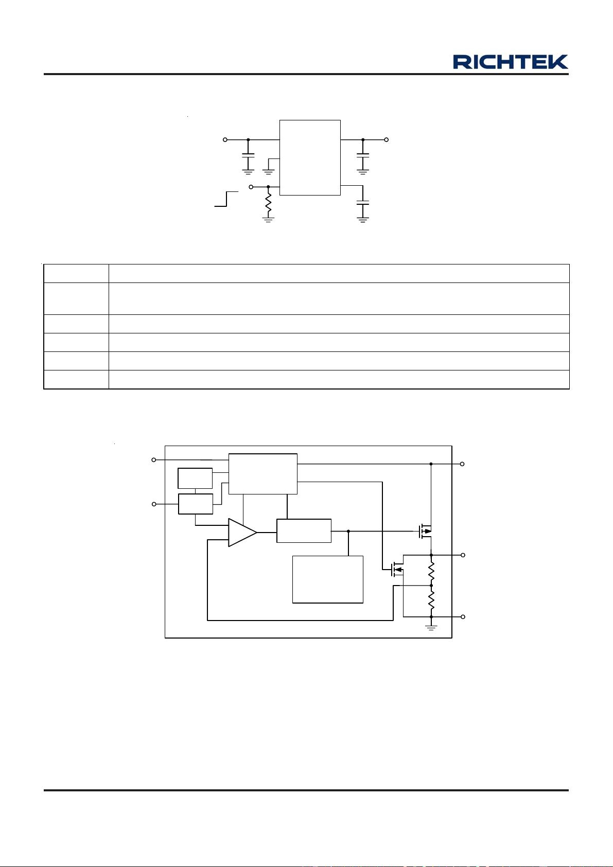
General Description
The RT9193 is designed for portable RF and wireless
applications with demanding performance and space
requirements. The RT9193 performance is optimized for
battery-powered systems to deliver ultra low noise and
low quiescent current. A noise bypass pin is available for
further reduction of output noise. Regulator ground current
increases only slightly in dropout, further prolonging the
battery life. The RT9193 also works with low-ESR ceramic
capacitors, reducing the amount of board space necessary
for power applications, critical in hand-he
ld wireless
devices. The RT9193 consumes less than 0.01μA in
shutdown mode and has fast turn-on time less than 50μs.
The other features include ultra low dropout voltage, high
output accuracy, current limiting protection, and high ripple
rejection ratio. Available in the 5-lead of SC-70, SOT-23
and WDFN-6L 2x2 packages.
Features
zz
zz
z
Ultra-Low-Noise for RF Application
zz
zz
z Ultra-Fast Response in Line/Load Transient
zz
zz
z Quick Start-Up (Typically 50
μμ
μμ
μs)
zz
zz
z < 0.01
μμ
μμ
μA Standby Current When Shutdown
zz
zz
z Low Dropout : 220mV @ 300mA
zz
zz
z Wide Operating Voltage Ranges : 2.5V to 5.5V
zz
zz
z TTL-Logic-Controlled Shutdown Input
zz
zz
z Low Temperature Coefficient
zz
zz
z Current Limiting Protection
zz
zz
z Thermal Shutdown Protection
zz
zz
z Only 1
μμ
μμ
μF Output Capacitor Required for Stability
zz
zz
z High Power Supply Rejection Ratio
zz
zz
z Custom Voltage Available
zz
zz
z RoHS Compliant and 100% Lead (Pb)-Free
Applications
z CDMA/GSM Cellular Handsets
z Battery-Powered Equipment
z Laptop, Palmtops, Notebook Computers
z Hand-Held Instruments
z PCMCIA Cards
z Portable Information Appliances
Note :
RichTek Pb-free and Green products are :
`RoHS compliant and compatible with the current require-
ments of IPC/JEDEC J-STD-020.
`Suitable for use in SnPb or Pb-free soldering processes.
`100% matte tin (Sn) plating.
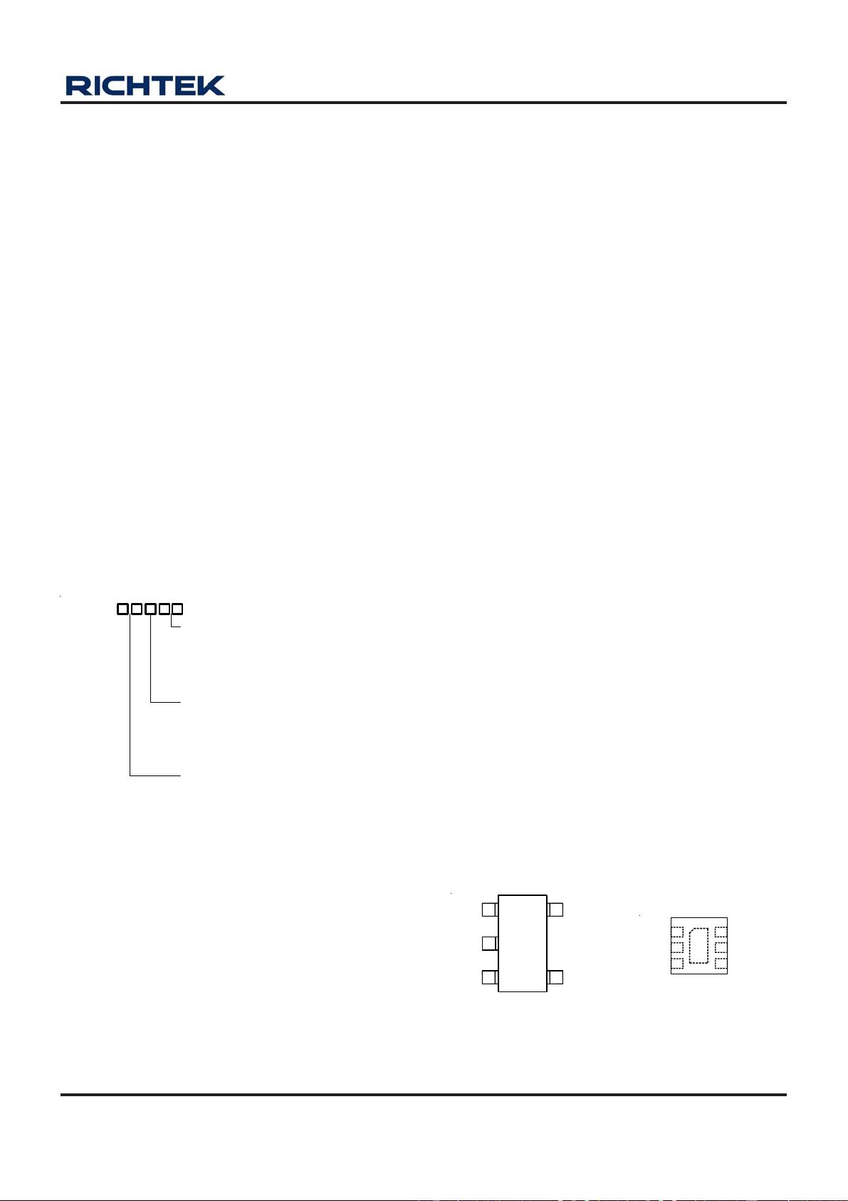
Pin Configurations
(TOP VIEW)
SC-70-5/SOT-23-5 WDFN-6L 2x2
VIN
GND
BP
VOUT
EN
2
3
5
4
1
EN
GND
BP
NC
VOUTVIN
5
4
1
2
3
6
RT9193-
Package Type
U5 : SC-70-5
B : SOT-23-5
QW : WDFN-6L 2x2 (W-Type)
Output Voltage
15 : 1.5V
16 : 1.6V
:
49 : 4.9V
50 : 5.0V
1H : 1.85V
2H : 2.85V
4G : 4.75V
Operating Temperature Range
P : Pb Free with Commercial Standard
G : Green (Halogen Free with Commer-
cial Standard)
RT9193
2
DS9193-09 March 2007www.richtek.com
Function Block Diagram
Functional Pin Description
Pin Name Pin Function
EN
Chip Enable (Active High). Note that this pin is high impedance. There should be a pull low 100kΩ
resistor connected to GND when the control signal is floating.
BP
Reference Noise Bypass
GND Ground
VOUT Output Voltage
VIN Power Input Voltage
Typical Application Circuit
Current-Limit
and
Thermal
Protection
MOS Driver
+
-
VOUT
Shutdown
and
Logic Control
VIN
Error
Amplifier
V
REF
BP
EN
GND
Quick
Start
VIN
GND
VOUT
RT9193
C
OUT
1uF/X7R
C
IN
1uF/X7R
V
IN
V
OUT
EN BP
C
BP
22nF
Chip Enable
RT9193
3
DS9193-09 March 2007 www.richtek.com
Electrical Characteristics
(V
IN
= V
OUT
+ 1V, C
IN
= C
OUT
= 1μF, C
BP
= 22nF, T
A
= 25°C, unless otherwise specified)
Parameter Symbol Test Conditions Min Typ Max Units
Output Voltage Accuracy ΔV
OUT
I
OUT
= 1mA −2 -- +2 %
Current Limit I
LIM
R
LOAD
= 1Ω 360 400 -- mA
Quiescent Current I
Q
V
EN
≥
1.2V,
I
OUT
= 0mA -- 90 130 μA
I
OUT
= 200mA, V
OUT
> 2.8V 170 200
Dropout Voltage (Note 5) V
DROP
I
OUT
= 300mA, V
OUT
> 2.8V -- 220 300
mV
Line Regulation ΔV
LINE
V
IN
= (V
OUT
+ 1V) to 5.5V,
I
OUT
= 1mA
-- -- 0.3 %
Load Regulation ΔV
LOAD
1mA < I
OUT
< 300mA -- -- 0.6 %
Standby Current I
STBY
V
EN
= GND, Shutdown -- 0.01 1 μA
EN Input Bias Current I
IBSD
V
EN
= GND or VIN -- 0 100 nA
Logic-Low Voltage
V
IL
V
IN
= 3V to 5.5V, Shutdown -- -- 0.4
EN Threshold
Logic-High Voltage
V
IH
V
IN
= 3V to 5.5V, Start-Up 1.2 -- --
V
Output Noise Voltage e
NO
10Hz to 100kHz, I
OUT
= 200mA
C
OUT
= 1μF
-- 100 -- μV
RMS
f = 100Hz -- −70 --
Power Supply
Rejection Rate
f = 10kHz
PSRR C
OUT
= 1μF, I
OUT
= 10mA
-- −50 --
dB
Thermal Shutdown Temperature T
SD
-- 165 -- °C
Absolute Maximum Ratings (Note 1)
z Supply Input Voltage ------------------------------------------------------------------------------------------------------ 6V
z Power Dissipation, P
D
@ T
A
= 25°C
SC-70-5 ---------------------------------------------------------------------------------------------------------------------- 300mW
SOT-23-5 -------------------------------------------------------------------------------------------------------------------- 400mW
WDFN-6L 2x2 -------------------------------------------------------------------------------------------------------------- 606mW
z Package Thermal Resistance (Note 4)
SOT-70-5, θ
JA
--------------------------------------------------------------------------------------------------------------- 333°C/W
SOT-23-5, θ
JA
--------------------------------------------------------------------------------------------------------------- 250°C/W
WDFN-6L 2x2, θ
JA
--------------------------------------------------------------------------------------------------------- 165°C/W
z Junction Temperature ----------------------------------------------------------------------------------------------------- 150°C
z Lead Temperature (Soldering, 10 sec.) ------------------------------------------------------------------------------- 260°C
z Storage Temperature Range -------------------------------------------------------------------------------------------- −65°C to 150°C
z ESD Susceptibility (Note 2)
HBM (Human Body Mode) ---------------------------------------------------------------------------------------------- 2kV
MM (Machine Mode) ------------------------------------------------------------------------------------------------------ 200V
Recommended Operating Conditions (Note 3)
z Supply Input Voltage ------------------------------------------------------------------------------------------------------ 2.5V to 5.5V
z EN Input Voltage ----------------------------------------------------------------------------------------------------------- 0V to 5.5V
z Junction Temperature Range --------------------------------------------------------------------------------------------
−40°C to 125°C
z Ambient Temperature Range --------------------------------------------------------------------------------------------
−40°C to 85°C
To be continued
剩余11页未读,继续阅读
Jacksware
- 粉丝: 0
- 资源: 22
上传资源 快速赚钱
- 我的内容管理 收起
- 我的资源 快来上传第一个资源
- 我的收益 登录查看自己的收益
- 我的积分 登录查看自己的积分
- 我的C币 登录后查看C币余额
- 我的收藏
- 我的下载
- 下载帮助
会员权益专享
最新资源
- 2023年中国辣条食品行业创新及消费需求洞察报告.pptx
- 2023年半导体行业20强品牌.pptx
- 2023年全球电力行业评论.pptx
- 2023年全球网络安全现状-劳动力资源和网络运营的全球发展新态势.pptx
- 毕业设计-基于单片机的液体密度检测系统设计.doc
- 家用清扫机器人设计.doc
- 基于VB+数据库SQL的教师信息管理系统设计与实现 计算机专业设计范文模板参考资料.pdf
- 官塘驿林场林防火(资源监管)“空天地人”四位一体监测系统方案.doc
- 基于专利语义表征的技术预见方法及其应用.docx
- 浅谈电子商务的现状及发展趋势学习总结.doc
- 基于单片机的智能仓库温湿度控制系统 (2).pdf
- 基于SSM框架知识产权管理系统 (2).pdf
- 9年终工作总结新年计划PPT模板.pptx
- Hytera海能达CH04L01 说明书.pdf
- 数据中心运维操作标准及流程.pdf
- 报告模板 -成本分析与报告培训之三.pptx
资源上传下载、课程学习等过程中有任何疑问或建议,欢迎提出宝贵意见哦~我们会及时处理!
点击此处反馈
安全验证
文档复制为VIP权益,开通VIP直接复制
信息提交成功
评论0