
Rev 0.1 / Jul. 2016 3
Preliminary
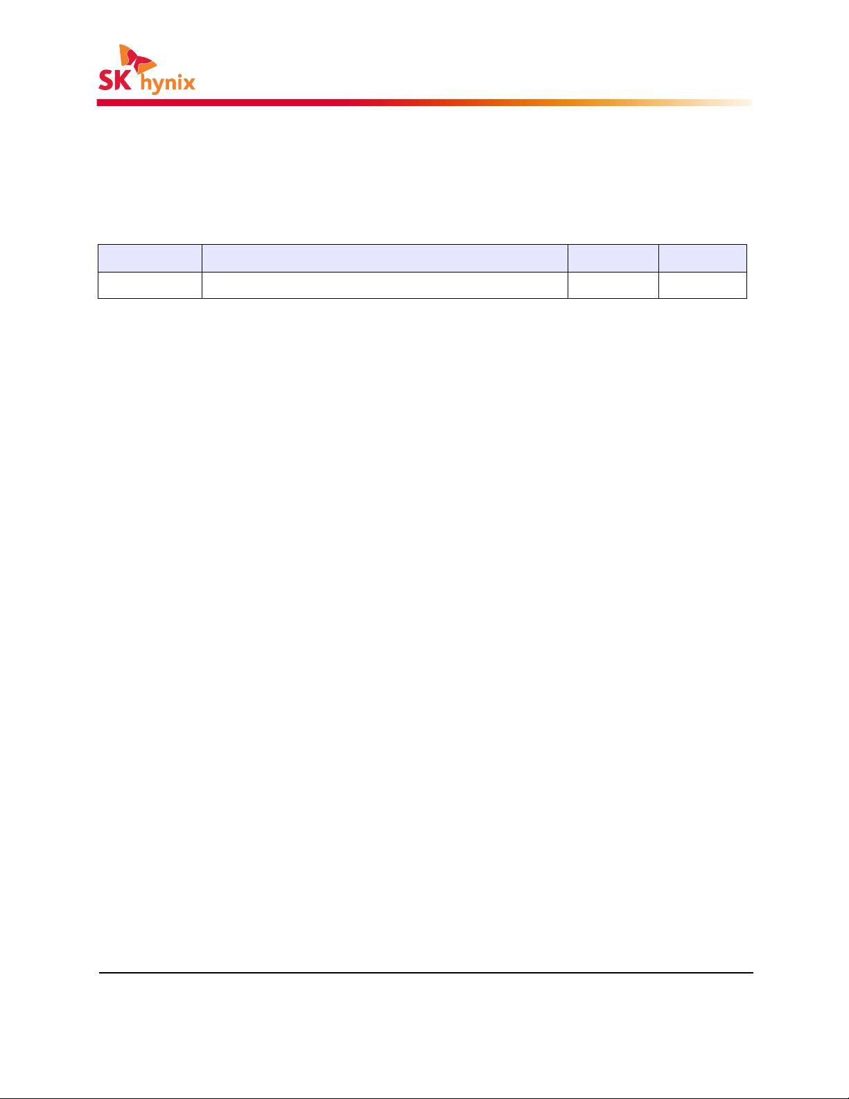
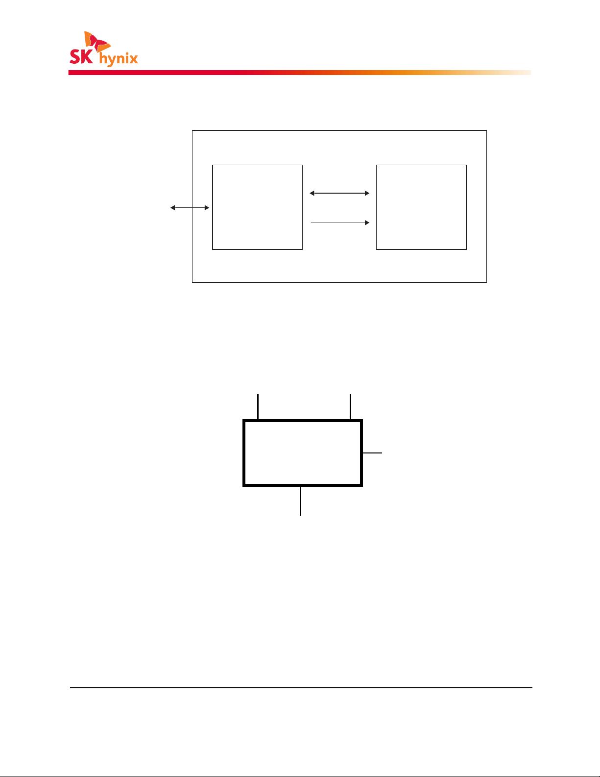
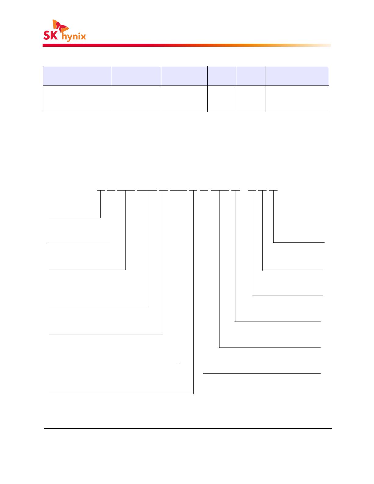
H9TQ64A8GTCCUR
8GB eMMC (x8) / LPDDR3 8Gb(x32)
FEATURES
[ eMCP ]
● Operation Temperature
- (-25)
o
C ~ 85
o
C
● Package
- 221-ball FBGA
- 11.5x13.0mm
2
, 1.0t, 0.5mm pitch
- Lead & Halogen Free
[ eMMC ]
• eMMC5.1 compatible
(Backward compatible to eMMC4.5&eMMC5.0)
• Bus mode
- Data bus width : 1 bit(default), 4 bits, 8 bits
- Data transfer rate: up to 400MB/s (HS400)
- MMC I/F Clock frequency : 0~200MHz
- MMC I/F Boot frequency : 0~52MHz
• Operating voltage range
-
V
cc
(NAND) : 2.7 - 3.6V
-
V
ccq
(Controller) : 1.7 - 1.95V / 2.7 - 3.6V
• Temperature
- Operation (-25
℃ ~ +85℃)
- Storage without operation (-40
℃ ~ +85℃)
• Others
- This product is compliance with the RoHS
directive
• Supported features
- HS400, HS200
- HPI, BKOPS, BKOP operation control
- Packed CMD, CMD queuing
- Cache, Cache barrier, Cache flushing
report
- Partitioning, RPMB, RPMB throughput improve
- Discard, Trim, Erase, Sanitize
- Write protect, Secure write protection
- Lock/Unlock
- PON, Sleep/Awake
- Reliable Write
- Boot feature, Boot partition
- HW/SW Reset
- Field Firmware Update
- Configurable driver strength
- Health(Smart) report
- Production state awareness
- Secure removal type
- Data Strobe pin, Enhanced data strobe
(Bold features are added in eMMC5.1)
[ LPDDR3 ]
• VDD1 = 1.8V (1.7V to 1.95V)
• VDD2 and VDDQ = 1.2V (1.14V to 1.30)
• HSUL_12 interface (High Speed Unterminated Logic 1.2V)
• Double data rate architecture for command, address and
data Bus;
- all control and address except CS_n, CKE latched at both
rising and falling edge of the clock
- CS_n, CKE latched at rising edge of the clock
- two data accesses per clock cycle
• Differential clock inputs (CK_t, CK_c)
• Bi-directional differential data strobe (DQS_t, DQS_c)
- Source synchronous data transaction aligned to bi-direc-
tional differential data strobe (DQS_t, DQS_c)
- Data outputs aligned to the edge of the data strobe
(DQS_t, DQS_c) when READ operation
- Data inputs aligned to the center of the data strobe
(DQS_t, DQS_c) when WRITE operation
• DM masks write data at the both rising and falling edge of
the data strobe
• Programmable RL (Read Latency) and WL (Write Latency)
• Programmable burst length: 8
• Auto refresh and self refresh supported
• All bank auto refresh and per bank auto refresh supported
• Auto TCSR (Temperature Compensated Self Refresh)
• PASR (Partial Array Self Refresh) by Bank Mask and Segment
Mask
• DS (Drive Strength)
• ZQ (Calibration)
• ODT (On Die Termination)


 我的内容管理
收起
我的内容管理
收起
 我的收益 登录查看自己的收益
 我的积分
登录查看自己的积分
我的积分
登录查看自己的积分
 我的C币
登录后查看C币余额
我的C币
登录后查看C币余额
 我的收藏
我的收藏  我的下载
我的下载  下载帮助
下载帮助 


评论0