MS-2374 Technical Article
Page 2 of 4
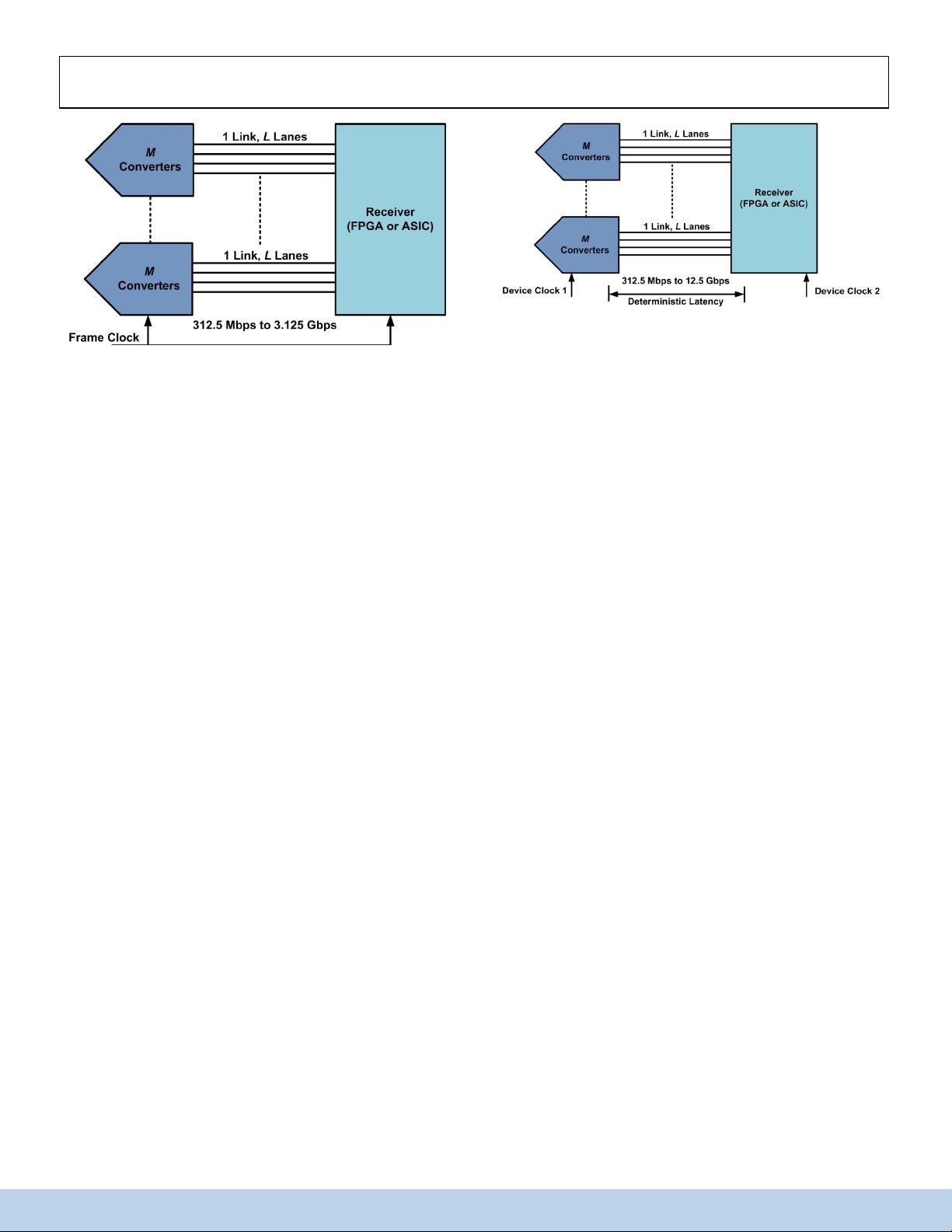
Figure 2. F
irst Revision—JESD204A
Although both the original JESD204 standard and the
revised JESD204A standard were higher performance than
legacy interfaces, they were still lacking a key element. This
missing element was deterministic latency in the serialized
data on the link. When dealing with a converter, it is important
to know the timing relationship between the sampled signal
and its digital representation in order to properly recreate
the sampled signal in the analog domain once the signal has
been received (this situation is, of course, for an ADC, a
similar situation is true for a DAC). This timing relationship
is affected by the latency of the converter which is defined
for an ADC as the number of clock cycles between the instant
of the sampling edge of the input signal until the time that its
digital representation is present at the converter’s outputs.
Similarly, in a DAC, the latency is defined as the number of
clock cycles between the time the digital signal is clocked
into the DAC until the analog output begins changing. In the
JESD204 and JESD204A standards, there were no defined
capabilities that would deterministically set the latency of
the converter and its serialized digital inputs/outputs. In
addition, converters were continuing to increase in both
speed and resolution. These factors led to the introduction
of the second revision of the standard, JESD204B.
In July of 2011, the second and current revision of the standard,
JESD204B, was released. One of the key components of the
revised standard was the addition of provisions to achieve
deterministic latency. In addition, the data rates supported
were pushed up to 12.5 Gbps, broken down into different
speed grades of devices. This revision of the standard calls
for the transition from using the frame clock as the main
clock source to using the device clock as the main clock
source. Figure 3 gives a representation of the additional
capabilities added by the JESD204B revision.
Figure 3. S
econd (Current) Revision—JESD204B
In the previous two versions of the JESD204 standard, there
were no provisions defined to ensure deterministic latency
through the interface. The JESD204B revision remedies this
issue by providing a mechanism to ensure that, from power-
up cycle to power-up cycle and across link re-synchronization
events, the latency should be repeatable and deterministic.
One way this is accomplished is by initiating the initial lane
alignment sequence in the converter(s) simultaneously across
all lanes at a well-defined moment in time by using an input
signal called SYNC~. Another implementation is to use the
SYSREF signal which is a newly defined signal for JESD204B.
The SYSREF signal acts as the master timing reference and
aligns all the internal dividers from device clocks as well as
the local multiframe clocks in each transmitter and receiver.
This helps to ensure deterministic latency through the system.
The JESD204B specification calls out three device subclasses:
Subclass 0—no support for deterministic latency, Subclass 1—
deterministic latency using SYSREF, and Subclass 2—
deterministic latency using SYNC~. Subclass 0 can simply
be compared to a JESD204A link. Subclass 1 is primarily
intended for converters operating at or above 500 MSPS
while Subclass 2 is primarily for converters operating below
500 MSPS.
In addition to the deterministic latency, the JESD204B version
increases the supported lane data rates to 12.5 Gbps and
divides devices into three different speed grades. The source
and load impedance is the same for all three speed grades
being defined as 100 Ω ±20%. The first speed grade aligns
with the lane data rates from the JESD204 and JESD204A
versions of the standard and defines the electrical interface
for lane data rates up to 3.125 Gbps. The second speed grade
in JESD204B defines the electrical interface for lane data
rates up to 6.375 Gbps. This speed grade lowers the minimum
differential voltage level to 400 mV peak-to-peak, down from
500 mV peak-to-peak for the first speed grade. The third
speed grade in JESD204B defines the electrical interface for
lane data rates up to 12.5 Gbps. This speed grade lowers the
minimum differential voltage level required for the electrical
interface to 360 mV peak-to-peak. As the lane data rates
increase for the speed grades, the minimum required
3
|
JESD204B Survival Guide


 我的内容管理
收起
我的内容管理
收起
 我的收益 登录查看自己的收益
 我的积分
登录查看自己的积分
我的积分
登录查看自己的积分
 我的C币
登录后查看C币余额
我的C币
登录后查看C币余额
 我的收藏
我的收藏  我的下载
我的下载  下载帮助
下载帮助 


评论0