没有合适的资源?快使用搜索试试~ 我知道了~
首页MALD-37030B_V2.pdf
资源详情
资源评论
资源推荐
MALD-37030B
MACOM Technology Solutions Inc. (MACOM) and its affiliates reserve the right to make changes to the product(s) or information contained herein without notice.
Visit www.macom.com for additional data sheets and product information.
For further information and support please visit:
https://www.macom.com/support
DC-0011245
1
26 Gbps Multi-Rate Laser Driver with Limiting Amplifier, Dual CDRs,
Power Management, and Diagnostics
Rev V2
Features
• DC coupled laser driver with up to 100mA bias and 76mA modulation current
• Internal buck-boost converter for automatic laser anode voltage optimization
• Reference-free TX and RX CDRs with bypass and multi-rate re-timing
• 25G & 21G VCO, half rate re-timing (MALD-37030)
• High input jitter tolerance with low output jitter
• Internal or external temperature sensor, supply voltage monitor, TX power
monitor, RSSI indicator
• Programmable AC or DC LOS threshold and slice level adjust on RX channel
• Integrated PRBS generator and checker and bidirectional loop back
• Integrated Fibre Channel RS0/RS1 rate select functionality
• Powered from a single 3.3V with internal 1.8V buck converter
• Supports -40 °C to +95 °C temperature range
MALD-37030 is a transceiver IC with dual CDRs targeted for long reach direct modulated Laser (DML) applications. The MALD-
37030 is intended for CPRI and 25G Ethernet telecom applications. The CDRs in the TX and RX channels are reference-free
and can be programmed to support half rate as well as bypassed to support legacy or non-standard data rates. The TX channel
includes a CTLE with adaptive/programmable equalization and a flexible output driver to directly drive DML lasers in TO-Cans
or in hybrid packages. A buck-boost converter tracks the laser forward voltage and automatically generates laser anode
voltages from 2.5V to 4.5V to optimize power dissipation and maintain eye quality. The RX channel includes a high-sensitivity
limiting amplifier with programmable peaking, slice level, LOS circuit with programmable threshold and hysteresis, a high
performance CDR with programmable loop bandwidth, and an output driver with programmable output swing and 2-tap de-
emphasis. The MALD-37030 is assembled in a 5 mm x 6 mm LGA (Land Grid Array) package and supports on-chip diagnostic
features like PRBS (31/9) generation, PRBS31 error detector and bi-directional loop-back. The device is controlled through an
I2C interface. The device is powered from a single 3.3V supply but an internal 1.8V buck converter supplies most of the chip
current.
Applications
• SFP28 Optical Modules
• Active Optical Cables
• 25-Gigabit Ethernet 25GbE
•CPRI
•SFP28
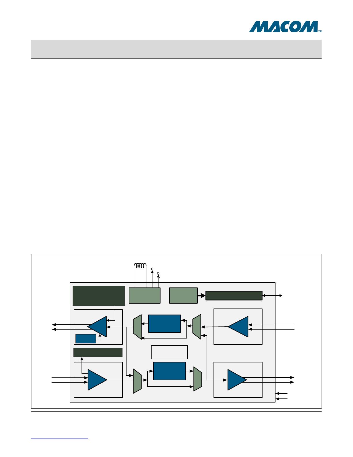
Functional Block Diagram
Programmable DE
and Output Swing
DRV
20G/25G/28G
CDR
with /2
Programmable LOS
And Slice Levels
Limit
Amp
CDR Bypass
Digital Interface
LOS Alarm
Output Buffer
Input Buffer
M
U
X
OUTIN
PRBS GEN /
CHECK
RS0
RS1
DML
DRV
20G/25G/28G
CDR
with /2
EQ
Output Buffer
Input Buffer
OUT
IN
M
U
X
CDR Bypass
Loop back
Tx Input
ROSA
Slave I2C
M
U
X
M
U
X
Loopback
Diagnostics
ADC
Power
Management
1.8V
Vanode
Laser power
control (SCL/OMA)
Eye adj.
TOSA
Rx Output
Ordering Information
Part Number Package Operating Temperature
MALD-37030B 5 x 6 mm, LGA package -40 to 95 °C
*MALD-37030 is RoHS compliant.
MALD-37030B
MACOM Technology Solutions Inc. (MACOM) and its affiliates reserve the right to make changes to the product(s) or information contained herein without notice.
Visit www.macom.com for additional data sheets and product information.
For further information and support please visit:
https://www.macom.com/support
DC-0011245
2
26 Gbps Multi-Rate Laser Driver with Limiting Amplifier, Dual CDRs,
Power Management, and Diagnostics
Rev V2
Revision History
Revision Level Date Description
V2 Release August 2018 Changed register 22h[6:4] to reserved in Ta bl e 5-1
Changed register 23h[4:0] to reserved in Ta bl e 5-1
Added RLASER_TRIM register use information in Section 3.1.2.3
Added Ibias and Imod overflow fault descriptions in Section 3.2.4.3
V1 Release June 2018 Split 37030B datasheet from 37030/1B combined datasheet
Removed 3.1.2.2.1 buck converter 1.7V output option
Updated Register 40h [5:4] in Section 4.0
Updated
JA,
JC
and R
LASER
in Table 1-2.
Removed P
T_ex
, P
de-emph
and P
T_exex
and updated footnote 5 in Tab le 1-3.
Updated R_TermIO, RX Tr/Tf, RX_TJ, TX Tr/Tf, T
X_TJ, TX_DJ, TX_DCD, TX_IJT, RX_CMN, I_MOD
LASER
resolution and I_BIAS
BASE
resolution in Table 1-4.
Removed footnote 18 in Tab le 1-4.
Updated default value of 1Eh, 1Fh, 20h, 21h, 22h from 00h to
xxh in Tab le 5-1.
Removed registers 47h, 48h, 49h and 4Ah in Tab le 4-1.
Removed VCO ranges from Features section.
Removed min and max values for 20G VCO in Table 1-4.
Added recommended inductor part numbers that are present between pins LI and LO and also between LX18 and
PM1
8
Updated VFAULTL and VFAULTH parameters in Table 1-5.
Updated Tab le 1-6.
Updated 41h, 80h - 8Fh in Section 4.0.
Updated Section 5.0.
Removed support for internal VCO PRBS generator option in Section 3.6.
Updated Reg 52h and added Reg C2h in Section
4.0.
Added TX Disable Section 3.2.1
Updated Section 3.2.4.2.1, Section 3.2.6.1, Section 3.2.6.2
MALD-37030B
MACOM Technology Solutions Inc. (MACOM) and its affiliates reserve the right to make changes to the product(s) or information contained herein without notice.
Visit www.macom.com for additional data sheets and product information.
For further information and support please visit:
https://www.macom.com/support
DC-0011245
3
26 Gbps Multi-Rate Laser Driver with Limiting Amplifier, Dual CDRs,
Power Management, and Diagnostics
Rev V2
V6P Preliminary October 2017 Added V
ESD,CDM
in Table 1-1.
Updated VCCR/VCCT typical spec. and SVCC max spec., removed low power mode, updated footnote 1 and added
footnotes 2, 3 to
Tab le 1-2.
Updated RX_VOUT spec, RX_Tr/Tf description, TX CTLE max for full rate, min for half rate, TX_IJT description and
note 6 in
Tab le 1-4.
Added t
PD
spec in Table 1-4.
Changed TX_IMOD and Imod symbol to I_MOD
LASER
, Tx_IDC to I_BIAS
BASE
and IMOD
laser
symbol to I_MOD
total
in
footnote 16 in
Tab le 1-4.
Updated V
OL_CMOS
max spec, V
OL_OD
max spec. in Tab le 1-5.
Updated I_BIAS
ave
equation in Section 3.2.4.1.
Added Figure 3-2.
Updated Section 3.1.1, Section 3.1.2.3.
Added configuration scripts to Section 3.6 and Section 3.7.
Removed Register 06h, 07h, 86h and 87h from Section 4.0.
Updated Register 20h [3], 22h [7], 25h [3:2], 33h [5:0], 45h [1], 63h, 78h [0], 52h[6] in Section 4.0.
Added Register 51h, 53h, 54h, 55h, 57h in Section 4.0.
Updated Registers 04h, 0Bh, 17h, 23h, 24h in Section 5.0.
V5P Preliminary July 2017 Change from Revision A to Revision B silicon and change the part number from MALD-37030A to MALD-37030B
and from MALD-37031A to MALD-37031B.
Update Marking Diagram Figure .
Update drawing of center pads in Figure 2-1.
Change Pin 40 definition to GNDPM in Figure 2-1 and Table 2-1.
Update package drawing in Figure 2-2.
Remove information on the 1.8V POR threshold in Ta ble 1-5 and Section 3.1.1.1. POR is only controlled by the
VCC33 supply in revision B silicon.
Correct reversed I2C Address instructions for READ and WRITE at 9Eh/9Fh and 98h/99h and correct 7 bit address
for Power Management registers from 4Eh to 4Fh in
Section 3.1.1 and all subsequent occurrences
Remove references to the password in the Initialization Procedure and remove the subsection describing the
password in
Section 3.1.1. It is not necessary to write the password in revision B silicon.
Provide more accurate approximations for the P0 and P1 laser currents in Section 3.2.4.1
Update description of TIA bandwidth control using the RSSI pin in Section 3.4.1.1.
Add reserved registers 0x06, 0x07, 0x33 - 0x38 and 0x44 and their default values to the register summaryTabl e 4-1
Update silicon revision ID in register 0x01, “Register Name: REVID” on page 45
Update settings for the TX Input CTLE at register 0x21, “Register Name: TX_ADAPT_EQ” on page 54
Change default setting of register 0x27h to C6h from C0h. Revision B part will default to TX disabled and will ignore
VCCT33 fault at TX_FAULT pin. See
“Register Name: LD_CTRL0” on page 56
Change default setting of register 4Ch.0x2C to 0Bh from 0Ah. Revision B part will initialize TX in Open Loop mode
instead of Single Closed Loop mode. See
“Register Name: OPMODE_CTRL” on page 58
Change the default value of register 4Ch.0x45[4] to 1b, “Register Name: DATA_OK” on page 64. Remove
instructions to write a value of 1b to this location in Section 3.1.2
Revision History
Revision Level Date Description
MALD-37030B
MACOM Technology Solutions Inc. (MACOM) and its affiliates reserve the right to make changes to the product(s) or information contained herein without notice.
Visit www.macom.com for additional data sheets and product information.
For further information and support please visit:
https://www.macom.com/support
DC-0011245
4
26 Gbps Multi-Rate Laser Driver with Limiting Amplifier, Dual CDRs,
Power Management, and Diagnostics
Rev V2
V4P Preliminary April 2017 Change VCC33 recommended operating voltage to 3.1V to 3.5V and remove note 2 in Tabl e 1-2
Increase SVCC (laser anode voltage) maximum to 4.5V in Table 1-2
Remove VCCR/T ripple and noise specification in Table 1-2
Add specification for P
de-emph
in Table 1-3
Update data rate retiming, JTBW, RTerm_LD, DCLOS
T_ASS
, DCLOS
T_DE-ASS
and TX_OFF specifications in
Table 1-4
Remove TXRX_ISO, Rx_PHA specification in Tab le 1-4
Add resolution and accuracy specification to TX_IMOD and TX_IDC in Tab le 1-4
Add typical values for 3.3V assert and de-assert to Table 1-5
Add Table 1-6 with Diagnostics specifications
Add Table 1-7 with I2C I/O specifications
Add Table 1-8 with I2C timing specifications
Change external filter requirements for Pin 36 (RSSI), update description of pin 38 (TSENSE), define pin 40 as a
GND pin, add capacitor recommendation to pin 41 (PVDDA) in
Tab le 2-1
Add information on revision B register password at Section 3.1.1.1
Information added on revision B POR operation at Section 3.1.1.1
Add instructions to write 4Ch.0x45[4]=1b at Section 3.1.2 and “Register Name: DATA_OK” on page 64
Add information on the switching frequency of the Buck and Buck-Boost converters in Section 3.1.2.2 and
Section 3.1.2.3 and correct capacitor connection to PMSVCC in Section 3.1.2.3
Update recommended Negative Current Limiter setting in Ta ble 3-2
Add information on setting the Buck converter output voltage to 1.7V in Section and “Register Name: TRIM_BYTE3”
on page 88
Correct reference to TX_FAULT pin (not TXDIS pin) in Section 3.1.2.4
Note added on TX path polarity in revision A and B in Section 3.2
Correct register address for IBIAS
base
in Section 3.2.4.1
Modify instructions on Tuning the TX output back termination at Section 3.2.4.2.1
Additional information added on MDIN pin functionality in Section 3.2.4.3.
Add instructions on operating in DOL, SCL and DCL in Section 3.2.6
Information added on Instant Start-up and Fast Start-up in Section 3.2.6.4 and Section 3.2.7
Information added on controlling ROSA bandwidth with pin RSSI in Section 3.4.1.1 and “Register Name:
ADC_CTRL3” on page 69
Add information on TX_FAULT pin at bit 6 of “Register Name: LB_MISCL” on page 46
Add TX_FAULT thresholds at registers “Register Name: TXFAULT_STATUS” on page 48and “Register Name:
LATCHED_STATUS” on page 48
Change bits 0x10[3], 0x20[3] and 0x43[7] to “reserved” at “Register Name: RX_MODES” on page 49 and “Register
Name: TX_MODES” on page 53 and “Register Name: LD_DRV_CTRL5” on page 64
Change “VCCT” to “VCC33” in description of register bits 4Ch.0x0A[3], 4Ch.0x0B[3] and 4Ch.0x27[1] in “Register
Name: TXFAULT_STATUS” on page 48, “Register Name: LATCHED_STATUS” on page 48 and “Register Name:
LD_CTRL0” on page 56.
Remove 15mV RxLOS threshold setting in “Register Name: RX_PKNG_LOS_THRS” on page 50
Change RX and TX CDR Loop Bandwidth settings and recommendations in “Register Name: RX_CDRLBW” on
page 51 and “Register Name: TX_CDRLBW” on page 55
Add information on TXLOS at “Register Name: TX_LOS_THRS” on page 54
Correct register 0x14 bit numbering at “Register Name: RX_CDR_MISCL” on page 52
Add details on TX eye shaping to “Register Name: LD_DRV_CTRL3” on page 63
Add description for tx_dcd to “Register Name: LD_DRV_CTRL4” on page 64
Correct description for im_msb andib_msb in “Register Name: i_msb” on page 72
Update undervoltage alarm thresholds at 4Fh.0x14[7:6] in “Register Name: ALARM_CTRL0” on page 78
Revision History
Revision Level Date Description
MALD-37030B
MACOM Technology Solutions Inc. (MACOM) and its affiliates reserve the right to make changes to the product(s) or information contained herein without notice.
Visit www.macom.com for additional data sheets and product information.
For further information and support please visit:
https://www.macom.com/support
DC-0011245
5
26 Gbps Multi-Rate Laser Driver with Limiting Amplifier, Dual CDRs,
Power Management, and Diagnostics
Rev V2
Marking Diagram
V3P Preliminary October 2016 Add POR thresholds for 1.8V and 3.3V supplies to Tabl e 1-5
Correct description of pin 23 (SVCC), add a requirement for ferrite isolation at pin 36 and update description of pins
41
and 45 in Table 2-1
Information added on initialization in Section 3.1.1
Information added on the 1.8V and laser anode buck-boost in Section 3.1.2
Information added on the TX
blocks in Section 3.2
Add Figure 3-3
Information added on OL, SCL and DCL control of lasers in Section 3.2.6
Add information on register 0x78 in Chapter 4
Add Power Management Register Table at Chapter 5
V2P Preliminary August 2016 Add marking diagram Figure
Change pin definitions of pins 21 - 24 in Figure 2-1
Correct pin numbering in Table 2-1
V1P Preliminary June 2016 Update specifications. Add register table.
V1A Advance March 2016 Initial Version
Revision History
Revision Level Date Description
剩余83页未读,继续阅读
Edmund19
- 粉丝: 9
- 资源: 25
上传资源 快速赚钱
- 我的内容管理 收起
- 我的资源 快来上传第一个资源
- 我的收益 登录查看自己的收益
- 我的积分 登录查看自己的积分
- 我的C币 登录后查看C币余额
- 我的收藏
- 我的下载
- 下载帮助
会员权益专享
最新资源
- 27页智慧街道信息化建设综合解决方案.pptx
- 计算机二级Ms-Office选择题汇总.doc
- 单链表的插入和删除实验报告 (2).docx
- 单链表的插入和删除实验报告.pdf
- 物联网智能终端项目设备管理方案.pdf
- 如何打造品牌的模式.doc
- 样式控制与页面布局.pdf
- 武汉理工Java实验报告(二).docx
- 2021线上新品消费趋势报告.pdf
- 第3章 Matlab中的矩阵及其运算.docx
- 基于Web的人力资源管理系统的必要性和可行性.doc
- 基于一阶倒立摆的matlab仿真实验.doc
- 速运公司物流管理模式研究教材
- 大数据与管理.pptx
- 单片机课程设计之步进电机.doc
- 大数据与数据挖掘.pptx
资源上传下载、课程学习等过程中有任何疑问或建议,欢迎提出宝贵意见哦~我们会及时处理!
点击此处反馈
安全验证
文档复制为VIP权益,开通VIP直接复制
信息提交成功
评论0