

Address Space
1-4
Introduction
1.4 Address Space
The MSP430 von-Neumann architecture has one address space shared with
special function registers (SFRs), peripherals, RAM, and Flash/ROM memory
as shown in Figure 1−2. See the device-specific data sheets for specific
memory maps. Code access are always performed on even addresses. Data
can be accessed as bytes or words.
The addressable memory space is 64 KB with future expansion planned.
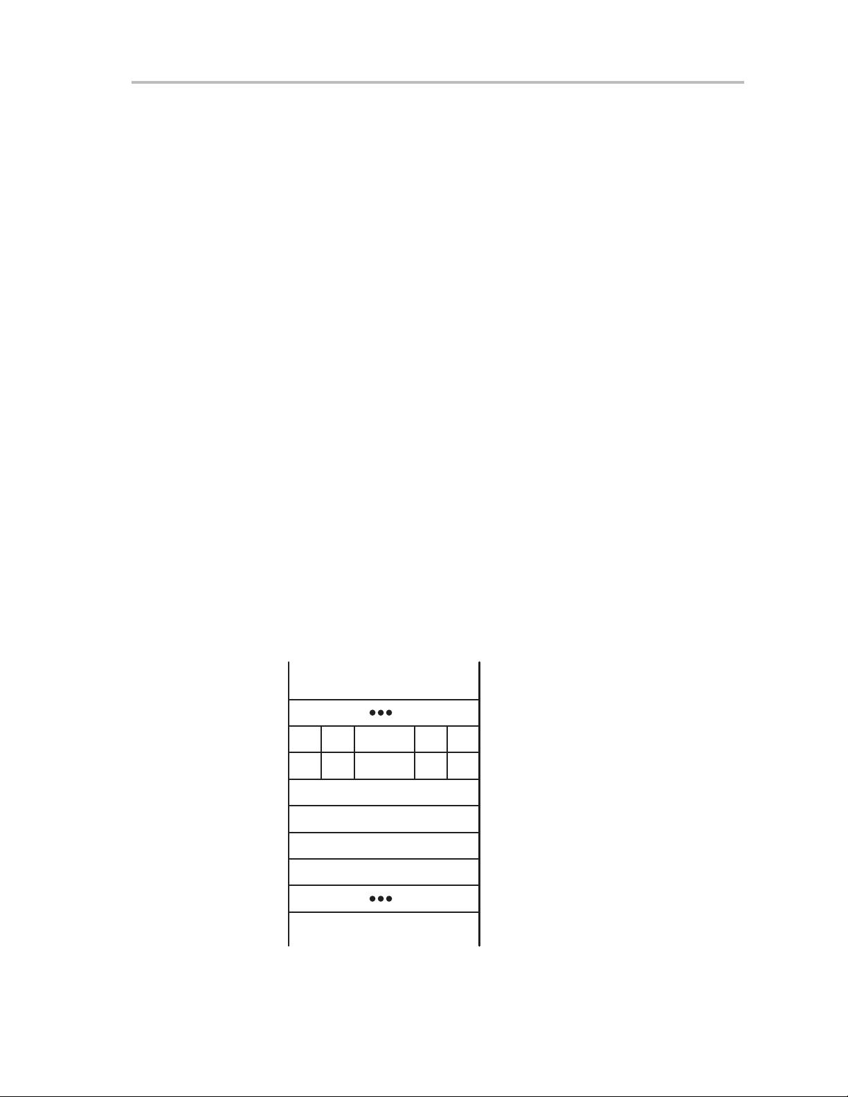
Figure 1−2. Memory Map
0FFE0h
Interrupt Vector Table
Flash/ROM
RAM
16-Bit Peripheral Modules
8-Bit Peripheral Modules
Special Function Registers
0FFFFh
0FFDFh
0200h
01FFh
0100h
0FFh
010h
0Fh
0h
Access
Word/Byte
Word/Byte
Word
Byte
Byte
Word/Byte
1.4.1 Flash/ROM
The start address of Flash/ROM depends on the amount of Flash/ROM
present and varies by device. The end address for Flash/ROM is 0FFFFh.
Flash can be used for both code and data. Word or byte tables can be stored
and used in Flash/ROM without the need to copy the tables to RAM before
using them.
The interrupt vector table is mapped into the upper 16 words of Flash/ROM
address space, with the highest priority interrupt vector at the highest
Flash/ROM word address (0FFFEh).
1.4.2 RAM
RAM starts at 0200h. The end address of RAM depends on the amount of RAM
present and varies by device. RAM can be used for both code and data.

剩余415页未读,继续阅读

selfsongs
- 粉丝: 128
- 资源: 20
 我的内容管理
收起
我的内容管理
收起
- 我的资源
快来上传第一个资源
 我的收益 登录查看自己的收益
 我的积分
登录查看自己的积分
我的积分
登录查看自己的积分
 我的C币
登录后查看C币余额
我的C币
登录后查看C币余额
 我的收藏
我的收藏  我的下载
我的下载  下载帮助
下载帮助

会员权益专享


最新资源
- VMP技术解析:Handle块优化与壳模板初始化
- C++ Primer 第四版更新:现代编程风格与标准库
- 计算机系统基础实验:缓冲区溢出攻击(Lab3)
- 中国结算网上业务平台:证券登记操作详解与常见问题
- FPGA驱动的五子棋博弈系统:加速与创新娱乐体验
- 多旋翼飞行器定点位置控制器设计实验
- 基于流量预测与潮汐效应的动态载频优化策略
- SQL练习:查询分析与高级操作
- 海底数据中心散热优化:从MATLAB到动态模拟
- 移动应用作业:MyDiaryBook - Google Material Design 日记APP
- Linux提权技术详解:从内核漏洞到Sudo配置错误
- 93分钟快速入门 LaTeX:从入门到实践
- 5G测试新挑战与罗德与施瓦茨解决方案
- EAS系统性能优化与故障诊断指南
- Java并发编程:JUC核心概念解析与应用
- 数据结构实验报告:基于不同存储结构的线性表和树实现
资源上传下载、课程学习等过程中有任何疑问或建议,欢迎提出宝贵意见哦~我们会及时处理!
点击此处反馈


